Study of Chromium Multilayers Properties Obtained by Pulsed Current Density: Residual Stress and Microhardness
Julieta TORRES-GONZÁLEZ1, Federico CASTAÑEDA1,*, Patrick BENABEN2
1 Centre for Research and Technological Development in Electrochemistry, Parque Tecnológico Querétaro Sanfandila 76703, Querétaro, México.
2 National School of Mines of Saint Etienne, 158 Cours Fauriel F-42023, Saint Etienne cedex 2, France.
E-mail: jtorres@cideteq.mx , *fcastaneda@cideteq.mx , benaben@emse.fr
*Corresponding author (Phone: +52 (442) 211 60 31, Fax: +52(442) 211 60 01)
Received: 22 July 2010 / Accepted: 23 December 2010 / Published: 24 December 2010
Abstract
Chromium multilayers deposits were obtained from three different bath solutions, they were prepared by switching current density between 10 and 70 Adm-2. Two temperatures were studied, 35°C and 55°C. At 35°C two different microstructures are alternated: columnar obtained at 10 Adm-2 and equiaxial obtained at 70 Adm-2. At 55°C only the columnar type microstructure is present, at 10 and 70 Adm-2, the only difference among the layers is a slight disorientation of grains. The properties of these chromium multilayers were characterized by scanning electron microscopy (SEM) and X-ray diffraction (XRD). In general the deposits are microcracked with a high microhardness, high residual stress and a small grain size.
Keywords:
Chromium multilayer coating; Pulse current density; Residual stress; Microhardness; Microstructure; Columnar; Equiaxial; Grain size
Introduction
Chromium deposits obtained from chromic acid solutions have a high microhardness, a good wear and corrosion resistance. These properties can be modified by the electrolyte composition and plating parameters such as temperature and current density [1].
Many studies have been done to improve the chromium properties, particularly corrosion resistance. As it is known, corrosion is influenced not only by the deposit thickness but also by the width and depth of cracks, in this sense cracks are influenced, among others things, by layer thickness, layer microstructure and residual stress.
Several methods are used to improve the physical properties of chromium deposits like: plasma nitriding [2], mechanical polishing [3], r.f. magnetron sputtering [4], pulsed-current electrolysis [5-10] with or without reversing polarity [11].
Varying the pulse frequency some authors found hardness values similar to those obtained by direct current plating, depending on the pulse frequency, hardness can be increased in 54 percent respect to the direct current plating [12]. Some of these methods try to modify the deposit surface [2, 3], while others try to avoid cracks development [4-11].
One of the approach to avoid cracks formation and by consequence to modify mechanical properties is to avoid stress accumulation and hence, crack development in consequence; maximum layer thickness must be stopped before to reach the critical stress value for crack appearance. In this sense, superposed thin chromium sublayers are a good option to try to obtain crack free deposits.
From this point of view, we have studied the chromium multilayers properties in particular electrodepositing alternated sublayers using two different current densities. In a previous study [13], we showed that deposits from standard and catalyzed baths at temperatures between 20 and 70ºC have mainly two types of microstructure, equiaxial and columnar. Each one of these microstructures has different mechanical and corrosion characteristics and is suitable as a departing point to obtain crack free chromium deposits.
In this paper we have chosen, 35°C as the lower temperature and 55°C as the higher temperature to obtain chromium multilayers, because it is the temperature range in chromium workshops. Indeed the purpose of this study is to produce multilayer chromium deposit alternating the two microstructures previously described and to characterize its physical properties, mainly residual stress, microstructure, grain size and microhardness.
Material and Method
Baths and Plating Conditions
Table 1 presents the different electrolytes used for the electrodeposition of chromium multilayers. Three baths have been tested, the standard bath, one commercial bath from Atotech, the so called HEEF25® and one mixed catalyst bath (SiF6).
Table 1. Chemical composition of used baths and plating conditions
|
|
Standard (gL-1) |
Mixed Catalyst (gL-1) |
aHEEF25® (Atotech) |
|
Cr203 |
250 |
250 |
Commercial |
|
SO42- |
2.5 |
0.6 |
Commercial |
|
SiF62- |
- |
10 |
Commercial |
|
Operating Conditions |
|||
|
Temperature °C |
35 and 55 ± 1 |
||
|
Cathodic current density (Adm-2) |
10 and 70 |
||
|
a A self-regulating high speed (SRHS) bath |
|||
Multilayers were obtained by alternating sublayers. The first sublayer was deposited at 10 Adm-2 then the following sublayer at 70 Adm-2 for both working temperatures used, i.e. 35 and 55°C. Temperature was thermostatically controlled to ± 1°C. Substrate used was carbon steel AISI 1018.
Two chromium sublayer thickness were studied, 1 and 0.2 μm. The plating time was set to obtain a 50 μm of total thickness comparable to hard chromium deposits.
The electrolytic cell was a 5-liters tank made of PTFE. Three shapes of the same carbon steel were used for the different analysis: a) Cylinders of about 1 cm in diameter and 7 cm long, b) parallelepipeds of about 0.9×0.9×2 cm and c) Plates of about 5×5×0.3 cm. The samples were mechanically polished and degreased in trichloromethane. Before electrodeposition the samples were anodically etched at a current density of 50 Adm-2 during 1 min in the same chromium plating solution. The anodes were made of a PbSbSn alloy (3% Sb and 3% Sn) and the shape was adapted to match the samples shape.
The cylindrical samples were cut along the longitudinal axe and polished mechanically for microhardness measures and etched in a modified Murakami's reagent [14] (100 gL-1 K3 [Fe (CN6)], 8 gL-1 NaOH, water) for the micrographic analysis.
Scanning Electron Microscopy (SEM), X Ray Difractommetry (XRD) and Microhardness
Several techniques were used to characterize the properties of the chromium layers. The microstructure was analyzed by SEM (JEOL 850), while grain size, crystallographic texture and residual stresses were determined by XRD. The diffractometer was composed of a Phillips goniometer coupled with a device called Dosophatex® (conceived at Ecole des Mines de Saint Etienne, France).
The measurements were achieved on the free surface of the chromium deposits. Pole figures were achieved on the surface of each sample. The {200} pole figures were obtained with the Co-Kα radiation. This peak is convenient due to its low multiplicity and good intensity. A calculus of X-ray penetration shows that in the case of chromium deposits, this penetration is around 1.2 μm.
The determination of residual stress was also carried out by XRD with the Co-Kα radiation (λKα= 1.785 Å) using the sin2θ method [15]. The measures were realized on the {211} planes due to its multiplicity (p=24) with a Bragg's angle (2θ = 98.88°) high enough for the precision of the measurements.
The chromium coatings microhardness was measured by a Vickers indenter (Matsuzawa MXT70) under a 15 sec, 100 g load on cross sections, perpendicular to the interface steel/chromium. The diagonals lines of the mark as well as the coatings thickness were measured by a computational program on a conventional optical microscope.
Results and Discussion
All chromium multilayers were started with a sublayer deposited at 10 Adm-2 and finished by a sublayer deposited at 70 Adm-2 All the multilayers from the three baths tested are well defined an separated as can be seen from SEM-FEG analysis, Figure 1a and 1b.
Chromium Sublayer Microstructure
1 μm sublayer thickness 35 °C
Figure 2a shows the structure of alternating 1 μm sublayers from Standard bath. We observe that chromium multilayers are microcraked; we can also see the formation of equiaxial grains at the interface substrate/deposit.
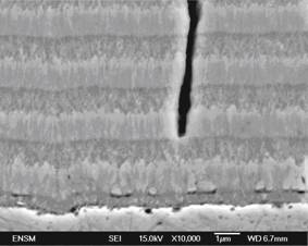
Figure 1a. SEM-FEG micrographs of bath1 μm Chromium multilayers from standard bath obtained at 55°C and 10-70 Adm-2
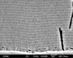
Figure 1b. SEM-FEG micrographs of 0.2 μm Chromium multilayers from SiF6 bath obtained at 55 °C and 10-70 Adm-2
There are some others equiaxial grains developed inside the sublayers in hazardous manner, these grains deform the continuity of subsequent sublayers producing columns emerging till surface giving a dull aspect to the deposit, Figure 2b. In spite of the very thin sublayer thickness (1µm), the cracks formed, cross the alternating sublayers and even, some of them, cross the entire multilayer thickness from substrate to surface. This behaviour is present only at 35°C, for the three baths tested and for 1 μm sublayer thickness (Micrographs for HEEF25® and mixed catalyst baths are not shown).
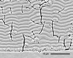
Figure 2a. SEM Micrographs of 1 μm chromium sublayer microstructure obtained from a standard bath at 35°C and 10-70 Adm-2
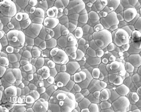
Figure 2b. Surface SEM Micrographs of 1 μm chromium sublayer obtained from a standard bath at 35 °C and 10-70 Adm-2
1 μm sublayer thickness 55 °C
At this temperature the alternated sublayer microstructures are both columnar for the three baths tested. The difference between them is a slightly grain disorientation. Figure 3a, 3b and 3c show the microstructure obtained from different baths. The 1 μm sublayers thicknesses are also microcracked and they are perpendicular to substrate. The deposits from SiF6 bath are the crackest with the lower crack size (see Table 2). It is evident that crack size is inversely proportional to crack density.
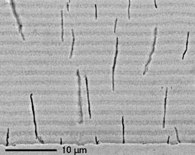
Figure 3a. SEM Micrographs of 1 μm chromium multilayers obtained from Standard bath at 55°C and 10-70 Adm-2
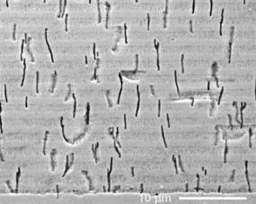
Figure 3b. SEM Micrographs of 1 μm chromium multilayers obtained from a SiF6 bath at 55°C and 10-70 Adm-2
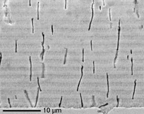
Figure 3c. SEM Micrographs of 1 μm chromium multilayers obtained from HEEF25® bath at 55 °C and 10-70 Adm-2
Table 2. Crack density and crack size for sinlge and multilayers
|
|
Standard |
|||||
|
|
Single Layer |
Alternated Sublayers |
||||
|
|
35°C |
55°C |
35°C |
55°C |
||
|
|
10 Adm-2 |
70 Adm-2 |
10 Adm-2 |
70 Adm-2 |
Alternating Sublayers |
|
|
Crack density (crack cm-2) |
1800 |
30 |
900 |
900 |
1200 |
900 |
|
Crack size ( μm) |
5 |
30 |
5 |
7 |
7 |
7 |
|
|
SiF6 |
|||||
|
Crack density crack dm-2 |
3500 |
30 |
1500 |
1500 |
1900 |
1500 |
|
Crack size μm |
2 |
30 |
5 |
5 |
3 |
5 |
|
|
HEEF25® |
|||||
|
Crack density crack dm-2 |
2100 |
30 |
200 |
200 |
800 |
2000 |
|
Crack size μm |
4 |
30 |
3 |
3 |
5 |
3 |
0.2 μm sublayer thickness 35°C
Figure 4a, 4b and 4c show the microstructures obtained from the three different baths at 35°C and for 0.2 μm sublayer thickness. As can be seen, the sublayers are microcracked, with some equiaxial grains. The quantity of equiaxial grains depends on the bath type.
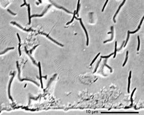
Figure 4a. SEM Micrographs of 0.2 μm chromium multilayers obtained from Standard bath at 35°C and 10-70 Adm-2
Deposits from standard bath present cracks deflected from the normal to substrate while deposits from SiF6 bath show that cracks are perpendicular to the substrate and the presence of equiaxial grains is almost zero. Deposits obtained from HEEF25® bath presents a lot of equiaxial grains and less cracks than for the others baths (see Table 2), again SiF6 bath is the crackest. No macrocracks i.e. cracks that crosses the entire layer from substrate to surface, are detected under experimental conditions for these three baths.
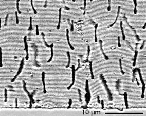
Figure 4b. SEM Micrographs of 0.2 μm chromium multilayers obtained from SiF6 bath at 35°C and 10-70 Adm-2
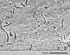
Figure 4c. SEM Micrographs of 0.2 μm chromium multilayers obtained from HEEF25® bath at 35 °C and 10-70 Adm-2
0.2 μm sublayer thickness 55°C
At 55° C and 0.2μm sublayer thickness the crack density in deposits from Standard bath decrease but they become longer, the deposits from the SiF6 bath exhibit more cracks than standard bath but HEEF25® is the crackest.
Here, again, the crack size increases as the crack density decreases, Figure 5a, 5b, 5c and Table 2.
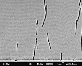
Figure 5a. SEM Micrographs of 0.2 μm chromium multilayers obtained from Standard bath at 55°C and 10-70 Adm-2
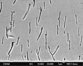
Figure 5b. SEM Micrographs of 0.2 μm chromium multilayers obtained from SiF6 bath at 55°C and 10-70 Adm-2
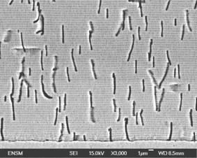
Figure 5c. SEM Micrographs of 0.2 μm chromium multilayers obtained from HEEF25® bath at 55°C and 10-70 Adm-2
Grain size
Grain size was obtained by XRD using the method described above:
· 35°C As it is well known, single layer deposits obtained at 35°C and 10 Adm-2 have a columnar structure and small grain size of about 6-7 nm, in the other hand, single layer deposits prepared at 35°C and 70 Adm-2 have an equiaxial microstructure with a bigger grain size of about 10-15 nm. Surprisingly the grain size for multilayers deposits is always small i.e. 6-7 nm, in spite of temperature and current density, i.e. both sublayers have a small grain, see Table 3.
· 55°C Single layer deposits obtained at 55°C at 10 and 70 Adm-2 have small grain size and columnar microstructure, no surprise then in obtaining small grain size for multilayers under these conditions (Table 3).
Table 3. Grain size for single and multilayers
|
|
Standard |
|||||
|
|
Single Layer |
Alternated Sublayers |
||||
|
|
35°C |
55°C |
35°C |
55°C |
||
|
|
10 Adm-2 |
70 Adm-2 |
10 Adm-2 |
70 Adm-2 |
Alternating sublayers |
|
|
Grain size nm |
7 |
15 |
7 |
7 |
7 |
7 |
|
|
SiF6 |
|||||
|
Grain size nm |
6 |
10 |
6 |
6 |
6 |
6 |
|
|
HEEF25® |
|||||
|
Grain size nm |
6 |
14 |
6 |
6 |
8 |
6 |
Residual stress
XRD is a well-known method for evaluating the residual stress however, even if the elastic coefficients values of the isotropic chromium (E=279 GPa, n=0.21) are taken into account, the results may well be different from the real values due to the microstructure and grain distribution anisotropy.
· 35°C The residual stress of the single layer deposits obtained at 35°C and 10 Adm-2 with columnar microstructure is high having a value of about ~1000 MPa. The residual stress for single layer deposits obtained at 35°C and 70 Adm-2 with equiaxial structure are negligible having a value of about 200-300 MPa. Nevertheless for multilayers, deposits obtained at 35°C regardless of current density, residual stress decreases as the presence of equiaxial grains becomes predominant. For standard bath the residual stress is around 750 MPa, for SiF6 deposits they are around 1000 MPa and for the HEEF25® they are inferior to 500 MPa (Table 4).
· 55°C Residual stress is high for the columnar microstructure obtained at 55° regardless of current density, with a value of 1000 MPa (see Table 4). So for multilayers obtained at 55 °C the residual stress is always high (~ 1000 MPa).
Table 4. Residual stress for single and multilayers
|
|
Standard |
|||||
|
|
Single Layer |
Alternated Sublayers |
||||
|
|
35°C |
55°C |
35°C |
55°C |
||
|
|
10 Adm-2 |
70 Adm-2 |
10 Adm-2 |
70 Adm-2 |
Alternating Sublayers |
|
|
Residual Stress Mpa |
1100 |
200 |
1000 |
1000 |
750 |
1000 |
|
|
SiF6 |
|||||
|
Residual Stress Mpa |
1000 |
300 |
1100 |
1100 |
1000 |
1100 |
|
|
HEEF25® |
|||||
|
Residual Stress Mpa |
1300 |
200 |
1100 |
1100 |
500 |
1100 |
Microhardness
· 35°C Regarding microhardness, single deposits obtained at 35°C at 10 Adm-2 having columnar microstructure also have a high microhardness. Deposits microhardness from standard bath is around 900, that of SiF6 baths is 1000 and that of HEEF25® is 950 HV100. Single deposits obtained at 35°C at 70 Adm-2 have equiaxial microstructure and have a low microhardness. Deposits from standard bath is around 600 HV100, that of SiF6 baths is around 800 HV100 and that of HEEF25® is around 700 HV100. Those with columnar microstructure have a higher microhardness about 1000 HV100 (Table 5).
Table 5. Vickers microhardness (HV100) for single and multilayers
|
|
Standard |
|||||
|
|
Single Layer |
Alternated Sublayers |
||||
|
|
35°C |
55°C |
35°C |
55°C |
||
|
|
10 Adm-2 |
70 Adm-2 |
10 Adm-2 |
70 Adm-2 |
Alternating sublayers |
|
|
Hardness HV100 |
900 |
600 |
950 |
950 |
1100 |
950 |
|
|
SiF6 |
|||||
|
Hardness HV100 |
1000 |
800 |
1000 |
1000 |
1100 |
1000 |
|
|
HEEF25® |
|||||
|
Hardness HV100 |
950 |
700 |
1100 |
1100 |
900 |
1100 |
Again, surprisingly, multilayer deposits obtained at 35° C have high microhardness value regardless of current density. Deposits from Standard and SiF6 bath have a microhardness of about 1000 HV100), those from HEEF25® bath are slightly lower 900 HV100 (Table 5).
· 55°C In the case of single layer deposits at 55°C at 10 and 70 Adm-2 the microhardness is high around, 1000 HV100. Consequently the hardness of multilayer deposits, as expected, is also high (1000 HV100). At this temperature deposits from HEEF25® have a slightly higher microhardness than the others (1100 HV100), see Table 5.
Conclusions
This study demonstrates that multilayer deposits have a different behaviour depending on the type of microstructure. Indeed the multilayers deposits have exactly the inverse characteristics than single layer deposits at 35°C and 70 Adm-2. When we obtain high microhardness in single layer deposits, we obtain low microhardness in multilayer deposits and so on for crack size, crack density, residual stress and grain size.
Surprisingly the grain size for multilayers deposits is always small i.e. 6-7 nm, in spite of temperature and current density, both sublayers have a small grain. Moreover for multilayers, deposits obtained at 35°C regardless of current density, residual stress decreases as the presence of equiaxial grains becomes predominant. For standard bath the residual stress is around 750 MPa, for SiF6 deposits is around 1000 MPa and for the HEEF25® is inferior to 500 MPa.
Again, surprisingly, multilayer deposits obtained at 35° C regardless of current density have high microhardness value. Deposits from Standard and SiF6 bath have a microhardness of about 1000 HV100). Hardness for deposits from HEEF25® bath are slightly lower (900 HV100).
Acknowledgements
The authors thank to Ciencia Básica 2005 - CONACyT, No. 48332 for the financial support and to ENSMSE, France and Centro de Investigación y Desarrollo Tecnológico en Electroquímica S.C to develop this research.
References
1. Torres-González J., Castaneda, F. and Benaben, P.,Characterization of physico-chemical properties of chromium electrodeposits, Theoretical and experimental advances in electrodeposition (ed. Luis Humberto Mendoza Huizar), India, Research Signpost, 2008,. p. 101-121.
2. Ge J.P., The effects of plasma nitriding on the structure and properties of electrodeposited chromium film, Plat. and Surf. Fin., 1996, 83(5), p. 146-148.
3. Hoshino S., Midorikawa T., Improvement of corrosion resistance of hard chromium plated articles by mechanical polishing and its mechanism, Ecole Nationale Superieure des Mines, St. Etienne, April 1998, p. 186-191.
4. Romero J., Lousa A., Martínez E., Esteve J., Nanometric chromium/chromium carbide multilayers for tribological applications, Surf. and Coat. Tech., 2003, 163-164, p. 392-397.
5. Pearson T., Dennis K., Effect of pulsed current on the properties of electrodeposited chromium, Plat. and Surf. Fin., Nov 1989, 76, p. 64-69.
6. Chai J.H., Chang D.Y., Kwon S.C., The properties of chromium electroplated with pulsed current, Plat. and Surf. Fin., 1989, 76, p. 80-82.
7. Gaigner G., Assoul M., Wery M., Pagetti J., Caractérisation tribologique des revêtements de chrome, Mat. et Tech., 2001, 11-12, p. 61-66.
8. Kobayashi Y., Nagasawa J., Watanabe K., Nakamura K., Sasaki T., Hirose Y., Contraintes résiduelles et propriétés thermiques des dépôts de chrome exempts de fissures obtenus par procédé électrolytique à courant pulse, Mat. et Tech., 2001, 11-12, p. 23-30.
9. Choi Y., Baik N.I., Hong S.I., Microstructural observation and wear properties of thin chrome layers prepared by pulse plating, Thin Solid Films, 2001, 397(1-2), p. 24-29.
10. Reby J., Vasseur G., Sutter B., Chromage dur en courant périodiquement inverse, 12th World Congress on Surface Finishing, Interfinish, 1988, AITE, Paris, p. 369-377.
11. Colombini C., Use of pulse rectifiers with periodic reversing polarity in hard chromium plating, 12th World Congress on Surface, Finishing Interfinish, 1988, AITE, Paris, p. 381.
12. Han S.H., Chang D.Y., Kwon S.C., Properties of pulsed-plated hard chromium from a self-regulating bath, Plat. and Surf. Fin., 1991, 78(9), p. 66-69.
13. Torres J., Benaben P., Study of the influence of electrolyte chemical composition on the properties of chromium electrodeposits: Microstructure, Crystallographic texture, Residual stress and Microhardness, Metal Finishing, 2003, 101(6), p. 107-116.
14. Portevin A., Bastien P., Réactifs d’attaque métallographique, Paris, Ed. Dunod, 1937.
15. Castex L., Lebrun J.L., Maeder G., Sprauel J.M, Détermination des contraintes résiduelles par diffraction de rayons X, Paris, ENSAM Publications Scientifiques et Techniques, 1981, 22, p 105-180.