VLSI System Implementation of 200 MHz, 8-bit, 90nm CMOS Arithmetic and Logic Unit (ALU) Processor Controller
Fazal NOORBASHA
Department Electronics and Communication Engineering, KL University, Vaddeswaram, Guntur (Dist.), A.P. (State), India - 522 502. E-mail: skfazalahmed@rediffmail.com
Corresponding author: Phone: +91-9000502785
Abstract
In this present study includes the Very Large Scale Integration (VLSI) system implementation of 200MHz, 8-bit, 90nm Complementary Metal Oxide Semiconductor (CMOS) Arithmetic and Logic Unit (ALU) processor control with logic gate design style and 0.12µm six metal 90nm CMOS fabrication technology. The system blocks and the behaviour are defined and the logical design is implemented in gate level in the design phase. Then, the logic circuits are simulated and the subunits are converted in to 90nm CMOS layout. Finally, in order to construct the VLSI system these units are placed in the floor plan and simulated with analog and digital, logic and switch level simulators. The results of the simulations indicates that the VLSI system can control different instructions which can divided into sub groups: transfer instructions, arithmetic and logic instructions, rotate and shift instructions, branch instructions, input/output instructions, control instructions. The data bus of the system is 16-bit. It runs at 200MHz, and operating power is 1.2V. In this paper, the parametric analysis of the system, the design steps and obtained results are explained.
Keywords
Very Large Scale Integration (VLSI); Complementary Metal Oxide Semiconductor (CMOS); Random Access Memory (RAM); Memory Address Register (MAR); Arithmetic and Logic Unit (ALU).
Introduction
The integrated circuit technology is the one of the most important fields of the electronics since it minimizes the area of the circuit, parasitic effects and the cost. Furthermore, these devices are more reliable than the circuits that are set up of the discrete components. Therefore, the interest in this subject is increasing day by day. There are many reports on microprocessor and ALU based electronic devices. Microprocessor is the main block for digital computer and some embedded systems. The technique learns in developing the simple machine will be useful when go for a full-fledged design in some higher-level. This presently developed simple system is improved the performance and working of the microprocessor signal management between the ALU and other peripherals [1].
Microprocessor applications encompass a wide range from high performance in system-on-a-chip (SOC) devices that supply networking, I/O processing, and modem banks, to power-consumption-limited personal digital assistants and cell phones. While the latter require increasing performance for increased functionality such as handwriting and voice recognition, low active and standby power consumption is the primary consideration for adequate battery life. The former applications, which are “tethered” or no battery powered, still desire low power but demand the highest possible performance. In these applications, low power enables greater integration and lower package cost due to improved thermal characteristics [2].
Arithmetic and Logic Unit (ALU) is circuit that can perform a large range of arithmetic and logic operations. Since the date is 8-bit long, we use an 8-bit ALU. The control input value decides the function ALU executes at a particular time. ALU can accept up to two operands at a time. But, ALU cannot perform multiply and division operation for which we use special hardware or some indirect technique [3]. Half of the above problem was solved in this system by developing a multiply circuit which is inbuilt in the ALU.
In the same way, now days all the devices and circuits are fabricated in VLSI System-On-Chip (SoC) Technology. In this study, a general-purpose 8-bit embedded ALU processor is designed using Very Large Scale Integrated Circuit (VLSI) design methods. The technology used to fabricate this design is 0.12µm, six metal CMOS technology. CMOS technology is preferred because of its low power dissipation and high integration density. Furthermore, the symmetrical structure of CMOS makes the design easier [4]. The design style of the integrated circuit is logic gate design style that includes some basic architecture such as transistors, gates and in order to construct a circuit designer makes interconnections between these units. Therefore, the design time that will be consumed for the system is minimized.
In this present work an ALU processor system was implemented and simulated. For system layout design, we have used 90nm CMOS technology. The operating frequency was 200 MHz and the data size was 8-bit. Here we have simulated eight arithmetic and logic operations. And the parametric analysis of the system, the design steps and obtained results are explained.
Material and Method
VLSI System Operation
In this VLSI system we are used embedded control units for ALU operations control. An embedded processor can be programmed to interact with different pieces of hardware. In this system, a memory called control memory holds the microinstructions that would produce the control signals for the microoprerations. The microoprerations are the operations that are executed by the subunits of the embedded system. The architecture of the embedded system is bus oriented which means that it has a main data bus that connects all the subunits. Thus, the data flow among the subunits is faster than a microcontroller that has a unidirectional bus [5]. Basically, the subunits of the embedded system can be grouped in to four main blocks. These are processing unit, memory unit, input-output unit and timing and control unit as shown in figure 1. The processing unit consists of arithmetic and logic unit (ALU), two data registers X and Y. The memory unit includes memory address register (MAR), Random Access Memory (RAM) row decoder and RAM block. The memory address register is four bits wide and latches the internal RAM address from the bus in order to read from or write to memory. RAM block consists of a 3-to-8 decoder and 8x8 bit static memory cells. The input-output unit provides the connection between the internal bus and the external buses. Finally, the timing & control unit produces the necessary signal for the proper operation of the embedded system controller [6]. The designed embedded system can perform the following types of instructions: transfer, arithmetic, logic, rotate, shift, input-output and control instructions.
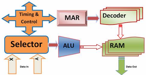
Figure 1. Functional Block Diagram of VLSI ALU Processor Control System
The operations of the embedded system can be explained in the following way: the instructions are read from the external data bus and the input latch, Din. Then, the instruction is decoded by MAR logic circuitry and the control unit produces control signals for the microoperations. Additionally, the bus control logic controls the access of the subunits to internal data bus. After decoding, one of the possible operations is followed according to the type of the instruction. The desired operation is performed upon the operand in the processing unit and finally the result is written into the destination. For output instructions, the data is transferred to the out of the embedded RAM through data output latch Dout and I/O port.
Design of Embedded System
Low-power embedded processors are used in a wide variety of applications, the reason for their wide use is that embedded processors are small; therefore, they do not take up much die area and are cheap to fabricate. Also embedded processors are verified, eliminating the need to spend additional engineering man-hours tracking down hardware flaws. Another great advantage in using embedded processors is that they run software, which enables one to deal with changing specifications as various system requirements change.
The regularity is a key factor in the design. By finding a standard cell, the desired function is implemented replicating these cells. Therefore, in this design, the leaf cells are searched and realized as a first step. After the simulation of the standard cells they are connected to build the subsystem units if the results are acceptable. Finally, the subsystem is simulated. In this section the design steps and the results will be introduced.
Processing Unit
The processing unit is the unit that achieves data manipulations on the operands. These operations can be transfer, arithmetic, logic and shift operations. The subunits of the processing unit are the arithmetic and logic unit and data registers. This 8-bit ALU is designed for different output results like – addition, subtraction, multiplication, 1’s complement, 2’s complement, increment by 1, decrement by 1 and comparison. Selector (Sel) is used for select the one of two 8-bit input data for ALU to do logical operations – i.e., 1’s complement, 2’s complement, increment by 1 and decrement by 1.The ALU unit mainly consists of multiplexers, half adders, full adders and some other logic gates. By using these devices total ALU is successfully designed and operations are successfully performed. This ALU perform the operations between two 8-bit input data and it can also perform the 4-bit multiplication operation successfully. Finally, the results of ALU are stored in embedded 8x8 RAM. The data registers X and Y are used to hold the operands for ALU operations. The basic elements of the registers are memory cells, consisting two inverters and two transmission gates.
The selector unit is mainly consists of multiplexers. This unit is useful to select one of the 8-bit input data from ‘X’ or ‘Y’. If the selector mode is set as ‘0’ it allows the 8-bit data ‘X’, if it is set as ‘1’ it allows the 8-bit data ‘Y’. This selected data is feed to the ALU for logical operations like 1’s complement, 2’s complement, increment by 1, and decrement by 1. The shifter having parallel loading, left shift, right shift and rotate capability is used for shift and rotate instructions. It is constructed using D-type flip flops and logic gates.
Memory Unit
It is designed to store necessary bits that can be changed during system operation and program flow. The memory unit includes 8x8 Static Random Access Memory (SRAM) matrixes; a 3-to-8 decoder and a memory address register (MAR). In the design phase of the RAM circuitry, first a static memory cell is designed. The cell includes cross-coupled two inverters and two pass transistors. Additionally, differential sense amplifier is prepared for reading operation. In order to select any one of the 8-bit row of the memory, MAR decodes the desired RAM location through the 3-to-8 row decoder which consisting logic gates. During read and write operations the memory address should be hold stable. For this purpose a register called memory address register is constructed of D-type flip flops.
Input-Output Unit
The input/output unit of the embedded system is used to provide an interface between the external world and the chip. This unit includes the data input and output latches and the port structure. The data input and output latches are used to store the data that is transferred between the external data bus and the internal bus.
Timing and Control Unit
The control unit is the unit that controls all the operations that are performed by the embedded system. Basically there are three elements of the control unit. These are the control address register, control memory and the ALU counter. The control memory is constructed of read only memory cells. The control decoder is similar to the memory address decoder and it used to address the rows of the control memory.
The control address register actually is a 4-bit width with parallel loading capability. It is designed using D type flip flops and logic gates. The control address register has 3 functions: reset for reaching the fetch commands in first rows of the control memory, incrementing to implement the next microoperation and loading for reaching to implement the next microoperation and loading for reaching opcodes of the fetched instruction.
Results and Discussion
The embedded chip units are fabricated in 0.12µm, 6-metal, 90nm CMOS process technology, with power supply 1.2V. The process characteristics and futures are shown in Table 1. The process is the result of several generations of development efforts directed towards high-performance microprocessors. The factors which drive process development for low-power design are similar to those which drive the process for pure high-performance although the motivation sometimes differs. For example, while both types of designs benefit from maximizing Idsat of the transistors at the lowest acceptable Vdd, the motivation for a pure high-performance design is reducing power distribution and thermal problems rather than extending battery life [6, 7]. Similar arguments apply to minimizing transistor leakage and on-chip variation of transistor parameters. This convergence of goals has been essential to our ability to develop one process to satisfy the requirements of both low-power and high-performance families. However, optimal voltage scaling algorithms are computationally expensive, and thus, if used online, significantly hamper the possible energy savings.
Table 1. 90nm Process Futures
|
Future Size |
0.12 µm |
|
Gate Oxide |
2.0 nm |
|
Power Supply |
1.2V |
|
Substrate |
P-epi. with n-well |
|
RAM Cell |
6 transistor |
|
Metal 1 width (µm) / space (µm) |
0.40/1.01 |
|
Metal 2 width (µm) / space (µm) |
0.40/2.01 |
|
Metal 3 width (µm) / space (µm) |
0.40/2.90 |
|
Metal 4 width (µm) / space (µm) |
0.40/3.80 |
|
Metal 5 width (µm) / space (µm) |
0.80/4.80 |
|
Metal 6 width (µm) / space (µm) |
0.80/6.00 |
|
Poly width (µm) / space (µm) |
0.20/0.01 |
|
Via width (µm) / space (µm) |
0.50/1.50 |
The SRAM memory arrays used in our designs employ conventional six-transistor SRAM cells with differential reads and writes. For memory reads and writes a 3-to-8 RAM decoder is designed and we have a single sense-amplifier per bit column. The main advantage of using a sense-amplifier on each bit-column is that it increases the amount of multiplexing required between the sense-amplifiers and the CPU [8, 9]. We developed the RAM Sense Amplifier CMOS Layout in 0.12µm technology. The width of the layout is 13.6µm, height is 23.3µm and total surf is 315.7µm2. To fabricate this RAM Sense Amplifier we have used 45 NMOS and 25 PMOS transistors. We have observed the voltage and current parametric analysis with respect to time (ns). The IddMax is 1.684mA, IddAvr is 0.008mA. We developed the 8x8 RAM CMOS layout in 0.12µm technology. The width of this layout is 19.7µm, height is 22.1µm and total surf is 434.5µm2. To fabricate this 8x16 RAM we have used 256 NMOS and 128 PMOS transistors. We have observed the voltage and current parametric analysis with respect to time (ns). The IddMax is 0.094mA, IddAvr is 0.004mA. We developed the 3-to-8 RAM Decoder CMOS Layout in 0.12µm technology. The width of the layout is 27.0µm, height is 6.8µm and total surf is 183.1µm2. To fabricate this 3-to-8 RAM Decoder we have used 35 NMOS and 35 PMOS transistors. We have observed the voltage and current parametric analysis with respect to time (ns). The IddMax is 0.995mA, IddAvr is 0.068mA. Voltage and Current analysis of 3-to-8 RAM Decoder is shown in figure 2. MAR RAM Row decoding timing and control results are shown in figure 3. Figure 4 shows the 90nm CMOS layouts of the RAM sense amplifier, 8x8 RAM and 3-to-8 RAM Row Decoder.
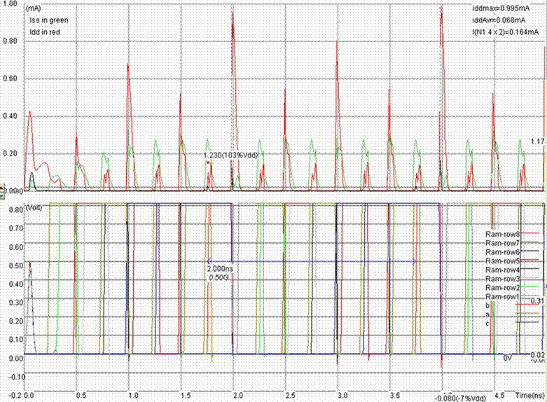
Figure 2. Voltage and Current Analysis of 3-to-8 Ram Row Decoder
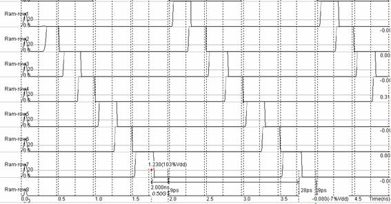
Figure 3. 3-to-8 RAM Row Data Decoder with MAR
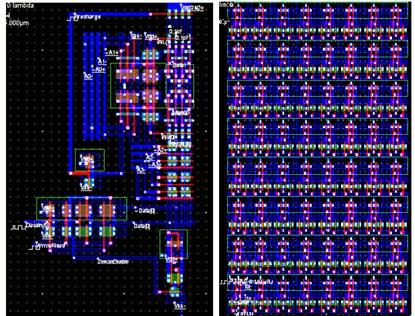
RAM Sense Amplifier 8×8 RAM
3-to-8 RAM Decoder
Figure 4. 90nm CMOS IC Layouts
We tested all the modules functionality properly and we have got expected results. We used two 8-bit data inputs X=00000101, Y=00000010 for checking the functionality of the embedded device. First of all we have stored the results of ALU i.e., arithmetic, logical and data transfer in the RAM. Then the memorized results are decoded according to our MAR address mode, by decoding the RAM rows through 3-to-8 decoder. Here in the results of subtraction and decrement by one, if the bit-4 is set as ‘0’ means positive signed result; else if it is set as ‘1’ means negative signed result. Here for all the ALU operations bit-4 is nothing but a carry bit except multiplication bit-7 is a carry bit. Here, if ‘sel’ is set as ‘0’ means logical operation is performing with the 8-bit data ‘X’, else with ‘Y’. The observed result waveforms are shown in the figure 5.
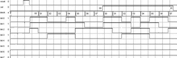
Figure 5. Decoding ALU results from RAM using MAR Address Decoder
Conclusions
A simple low-power and high-speed 8-bit ALU processor control VLSI system is implemented to improve microprocessor ALU operations performance. This system has designed and simulated successfully for its functionality. To develop this VLSI device, we used Cadence, Xilinx, Microwind and Modelsim softwares and tools. By giving the 4-bit code to the MAR, the user to select any type of microprocessor ALU operation result from RAM to give other peripherals synchronously. And it contains a multiplication operation circuit which was improving the microprocessor’s ALU performance. The technology used to fabricate this design is six metal 90nm CMOS technology. CMOS technology is preferred because of its low-power dissipation and high integration density. It runs at 200MHz, and operating power is 1.2V.
References
1. Andrei A., Eles P., Jovanovic O., Schmitz M., Ogniewski J., Peng Z., Quasi-Static Voltage Scaling for Energy Minimization With Time Constraints; IEEE Transactions on Very Large Scale Integration (VLSI) Systems, 2011, 19(1), p. 10-23.
2. Clark L.T., Hoffman E.J., Miller J., Biyani M., Liao Y., Strazdus S., Morrow M., Velarde K.E., Yarch M.A., An Embedded 32-b Microprocessor Core for Low-Power and High-Performance Applications; IEEE Journal of Solid-State Circuits, 2001, 36(11), p. 1599-1608.
3. Deleganes D.J., Barany M., Geannopoulos G., Kreitzer K., Morrise M., Milliron D., Singh A.N., Wijeratne S., Low-Voltage Swing Logic Circuits for a Pentium ® 4 Processor Integer Core; IEEE Journal of Solid-State Circuits, 2005, 40(1), p. 36-43.
4. Lei Zhang, Meikang Qiu, Edwin H.-M. Sha, Qingfeng Zhuge, Variable assignment and instruction scheduling for processor with multi-module memory; Microprocessors and Microsystems, 2011, 35(3), p. 308-317.
5. Satyanarayana N., Vinaya A, Babu A., Madhu Mutyam, Delay-efficient bus encoding techniques; Microprocessors and Microsystems, 2009, 33(5-6), p. 365-373.
6. Hritam Dutta, Dmitrij Kissler, Frank Hannig, Alexey Kupriyanov, Jürgen Teich, Bernard Pottier, A holistic approach for tightly coupled reconfigurable parallel processors ; Microprocessors and Microsystems, 2009, 33(1), p. 53-62.
7. Nojiri T., Kondo Y., Irie N., Ito M., Sasaki H., Maejima, H., Domain Partitioning Technology for Embedded Multicore Processors; Micro, IEEE, 2009, 29(6), p. 7-17.
8. Mudge T., Holzle U., Challenges and Opportunities for Extremely Energy-Efficient Processors; Micro, IEEE, 2010, 30(4), p. 20-24.
9. Devietti J., Lucia B., Ceze L., Oskin M., DMP: Deterministic Shared-Memory Multiprocessig; Micro, IEEE, 2010, 30(1), p. 40-49.