Modelling and Simulation of SVPWM Based Vector Controlled HVDC Light Systems
Ajay Kumar MOODADLA*, and Venkata Srikanth NANDIRAJU
Electrical Engineering Department, National Institute of Technology-Warangal, Andhra Pradesh, India
E-mail: ajaykumar.nitw@gmail.com
* Corresponding author: Phone: +91-9491827298
Abstract
Recent upgrades in power electronics technology have lead to the improvements of insulated gate bipolar transistor (IGBT) based Voltage source converter High voltage direct current (VSC HVDC) transmission systems. These are also commercially known as HVDC Light systems, which are popular in renewable, micro grid, and electric power systems. Out of different pulse width modulation (PWM) schemes, Space vector PWM (SVPWM) control scheme finds growing importance in power system applications because of its better dc bus utilization. In this paper, modelling of the converter is described, and SVPWM scheme is utilized to control the HVDC Light system in order to achieve better DC bus utilization, harmonic reduction, and for reduced power fluctuations. The simulations are carried out in the MATLAB/SIMULINK environment and the results are provided for steady state and dynamic conditions. Finally, the performance of SVPWM based vector controlled HVDC Light transmission system is compared with sinusoidal pulse width modulation (SPWM) based HVDC Light system in terms of output voltage and total harmonic distortion (THD).
Keywords
VSC HVDC; HVDC Light; Space vector PWM; Sinusoidal PWM.
Introduction
The conventional Line-commutated Current source Converter based HVDC (LCC-HVDC) transmission system is a power electronics technology used in power systems which can transmit large amount of power over long distances [1,2]. Due to advancement of power electronic technology, HVDC technology utilizes voltage source converters (VSC) with self-commutating IGBT converter valves and this technology is named as HVDC Light system [3-5]. The breakthrough was made when the world’s first IGBT technology based HVDC Light system was installed in March 1997 (Hellsjon project, Sweden, 3MW, ±10kV, 10km distance) [3]. Since then many HVDC Light systems have been installed worldwide [5].
The HVDC Light system is different from the Conventional HVDC system in many aspects. Specifically, Pulse Width Modulation (PWM) technique is used in the HVDC Light system to create any desired voltage waveform, any phase angle and magnitude of the fundamental frequency component. The HVDC Light transmission system has several benefits [6,7]:
· Since, IGBT can turn-off a current at any time, the HVDC Light system offers rapid and independent control of active and reactive power generated or consumed by the converters.
· The HVDC Light system provides a convenient and cost-effective way for connecting non-polluting and renewable energy sources to the main grid, with strong environmental benefits.
· The HVDC Light system allows the two converters to either generate or consume reactive power, to the AC side, and thus work as independent static VAR compensators on the AC sides.
· By eliminating the commutation failure problem, the HVDC Light system reduces the voltage dip and waveform distortions on the AC network.
· In the HVDC Light transmission system, without changing the polarity of the DC voltage, reversal of power flow can achieve by simply reversing the direction of DC current, and this feature is critical for all multi-terminal DC systems.
· By employing multi-level converter topologies, HVDC Light system inherently reduces the harmonics in the AC currents and voltages, and hence the size of the filters required is also small.
· With an excellent feature of the HVDC Light system so called “Black-start capability”, it can start up against a dead network.
Traditionally, both of the converters in the HVDC Light system are controlled by the pulses generated by Sinusoidal PWM (SPWM) scheme [8]. But the conventional SPWM has the limitations of incomplete utilization of dc bus voltage, high THD, and difficult to implement advanced vector control algorithms.
The main objective of this paper is to introduce SVPWM control in the HVDC Light transmission systems to overcome the above said drawbacks.
Principle of HVDC Light System
A typical HVDC Light transmission system is shown in figure 1. It consists of two identical neutral point clamped (NPC) VSC stations, which are linked with a DC cable. The main function of a transformer is to transform AC voltage into secondary voltage adapted to the DC link in the converter. Reactors are placed to secure the power exchanges between VSC and AC system. Filters are also introduced to absorb high frequency harmonics. Finally, the purpose of DC capacitors on the DC side on each converter as shown in figure 1 is to provide voltage support and harmonic attenuation.
|
|
|
Figure 1. Typical HVDC Light system |
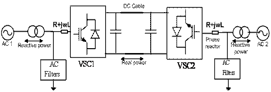
In figure 1 AC side and VSC side having the line-to-line AC bus voltage Vs and converter AC voltage Vc respectively, are interconnected by a DC cable with the reactance X. In steady state ignoring the harmonic components and resistance, the active power P, and reactive power Q absorbed by the VSC are given by the following relations:
|
P = (Vs*Vc)*sinδ/X |
(1) |
|
Q = Vs (Vs-Vc*cosδ)/X |
(2) |
where δ is the phase angle of the fundamental component of PWM. Thus, it is possible to control P and Q independently by δ and Vc, respectively. When VSC operates as a rectifier, the converter output AC voltage lags AC bus voltage by an angle δ; when VSC operates as an inverter, the converter output AC voltage leads by an angle δ.
Mathematical Modelling and Control
A plethora of excellent publications exists in the literature associated with the HVDC Light system, in the area of modelling and control. Each station in the HVDC Light system is coupled with AC network via line resistor R, phase reactor L and a DC capacitor C is in parallel to the DC bus of the station shown in figure 1. The following equations are obtained in the d-q synchronous frame [9,10]:
|
|
(3) |
|
|
(4) |
where Vsd and Vsq are source voltages, id and iq are line currents, Vcd and Vcq are converter input voltages.
Based on the instantaneous reactive theory, neglecting the losses of the converter and the transformer, the active and reactive power exchanges from the AC end of the DC link are:
|
Pac=3·(Vsd·id+Vsq·iq)/2 |
(5) |
|
Qac=3·(Vsd·iq-Vsq·id)/2 |
(6) |
Suppose, the direction of the source voltage vector as d-axis, Vsq =0. So (5) and (6) can be written as:
|
Pac=3·Vsd·id/2 |
(7) |
|
Qac = 3·Vsd·iq/2 |
(8) |
Since Vsd is constant, from (7) and (8) it is clear that the active power will be controlled by id, whole the reactive power will be controlled by iq.
On the DC side of the converter, DC current and DC power are:
|
|
(9) |
|
Pdc=Vdc·idc |
(10) |
Where idc is the DC current to be followed by the capacitor, Vdc is the DC link voltage and ic is the current on the DC cable. Neglecting the loss of converter, power of AC side equals to the DC side:
|
Pac=Pdc |
(11) |
|
3·Vsd·id/2= Vdc·idc |
(12) |
The AC voltage of VSC can be described as:
|
|
(13) |
where Vc is the converter ac voltage and, m is the modulation ratio. In general the converters are controlled through Sinusoidal PWM (SPWM), where the modulating signal is a sinusoidal one and the carrier signal is a triangular signal and the ratio between the two peak values is known as modulation ratio (m). But in the space vector PWM, modulation ratio m is given by:
|
|
(14) |
The value of m can be: 0≤ m ≤ 1.
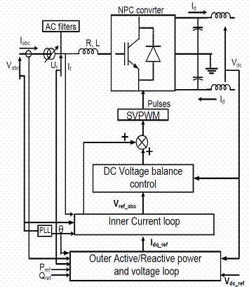
Figure 2 depicts an overall control structure of the NPC converter station and its interface with the main circuit. The station 1 and station 2 controller designs are identical. In the present case, controlled parameters are [11]:
· Active power (P) and Reactive power(Q) in station 1
· DC voltage (Vdc) and Reactive power(Q) in station 2.
The phase locked loop (PLL) block measures the system frequency and calculates the phase angle (θ ) for the dq transformation block. The active/reactive power and voltage loop block in figure 2 contains the outer loop regulators that calculate the reference value of the converter current vector ( Iref_dq), which is the input to the inner current loop.
The Inner current loop block contains two PI regulators that will calculate the reference value of the converter voltage vector (Vref_dq). By using clarke’s transformation Vref_dq is transformed into Vref_abc, which is the input to the space vector pulse width modulation (SVPWM). Due to inherent unbalance in the circuit components impedance, there may be some deviations in the DC side pole voltages. DC voltage balance control block is to maintain the dc side of the three level bridges balanced.
|
|
|
Figure 2. Overall control structure of converter station |
Space Vector PWM for Three-Level Converters
A three phase three level neutral point clamped (NPC) converter is shown in figure 3. It consists of 12 IGBT’s (4 on each leg) and also supplied with two capacitors to split the DC voltage into two, for providing the neutral point. Space vector pulse width modulation (SVPWM) scheme is a new concept for HVDC Light applications. It is based on the space vector representation of the voltages on the two phase coordinates [10]. Initially, using park’s transformation, three phase quantities are transformed into their equivalent two phase quantities either in the stationary or synchronously rotating frame, where the total power and impedances, are remains same. The resultant of these two components gives the Vref vector magnitude, which will decide the converter output.
The number of switching states for a three level NPC inverter is 27 and among them, 24 are active states and remaining 3 are zero states. If the switching state is 1, it means that upper two switches in leg A are connected, and the output voltage VAO is +Vdc. Similarly -1 indicates that lower two switches are ON, which means VAO= -Vdc. If the switching state is O, it resembles that inner two switches S2 and S3 are connected and VAO=0. Similar concept will exist for leg B and leg C. The switching states and their output voltage levels of three levels NPC inverter are given in table 1.
|
|
|
Figure 3. A three phase three-level NPC converter |
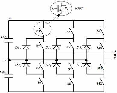
Table 1. Switching states and output voltage levels of three-level converter
|
VAO |
S1 |
S2 |
S3 |
S4 |
|
+Vdc |
1 |
1 |
0 |
0 |
|
0 |
0 |
1 |
1 |
0 |
|
-Vdc |
0 |
0 |
1 |
1 |
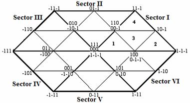
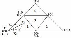
Space vector diagram of the three level inverter has been shown in figure 4, which is divided into the six sectors and each sector has four regions 1,2,3 and 4. The time duration of each voltage vector is calculated by volt-Sec balance equation as follows:
|
T1V1+T2V2+T3V3= TSVref |
(15) |
|
T1+T2+T3=TS |
(16) |
where V1, V2, and V3 are the three vectors that define the triangular region in which Vref is located. T1, T2 and T3 are the corresponding vector duration and Ts is the sampling time.
|
|
|
Figure 4. Space vector diagram of three-level converter |
Step by Step Algorithm for Realization of SVPWM
Step 1: Calculate Vd , Vq, Vref and the angle (α) by using park’s transformation.
Step 2:After calculating α, determine the sector depending on the position of Vref as shown in table 2.
Table 2. Sector calculation based on the location of Vref
|
Range of α (degree) |
0≤α <60 |
60≤α <120 |
120≤α <180 |
180≤α <240 |
240≤α<300 |
300≤α<360 |
|
Location of Vref |
Sector I |
Sector II |
Sector III |
Sector IV |
Sector V |
Sector VI |
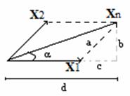
Step 3: Determine the region in the corresponding sector. To estimate the region in sector I, space vector diagram for X1 and X2 is shown in figure 5, and corresponding switching logic is given in table 3.
|
a) |
b) |
|
Figure 5. Space vector diagram for X1 and X2 in Sector I. |
|
|
|
(17) |
|
|
(18) |
Table 3. Logic used to find the region in which Vref is located
|
X1 and X2 |
Position of Vref |
|
X1 , X2 and (X1 + X2 ) < 0.5 |
Region 1 |
|
X2 > 0.5 |
Region 2 |
|
X1 > 0.5 |
Region 3 |
|
X1 and X2 < 0.5 and (X1 + X2 ) > 0.5 |
Region 4 |
Step 4:Determine the switching time of each switch in all the regions. Following equations gives the switching time in region 1:
|
|
(19) |
|
|
(20) |
|
|
(21) |
where m is modulation ratio and 0≤ α ≤ π/3.
Results
System data: AC systems 1 & 2: 100kV, 50 Hz, Smoothing reactor: 8mH; Grid-filter: 0.75Ω, 0.2H; DC line: ± 100kV, 100km; DC link capacitor: 70µF; Switching frequency: 1350 Hz.
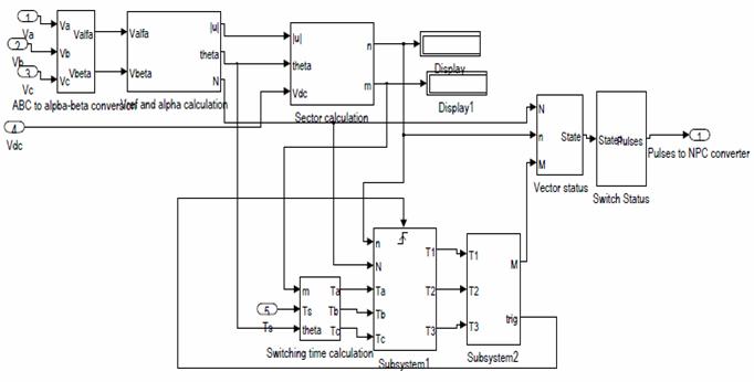
A complete simulation model is shown in figure 6, which gives the gating signals to both the converter stations independently. The operation of this control strategy in the HVDC Light transmission system was verified in a MATLAB/SIMULINK environment for a steady state, single phase to earth fault and three phase fault at t = 1.0 s.
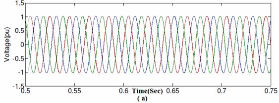
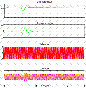
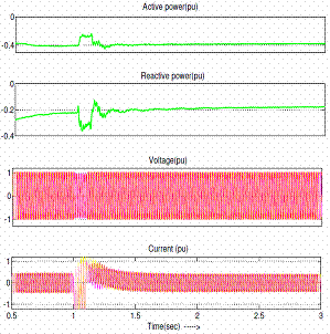
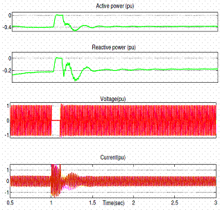
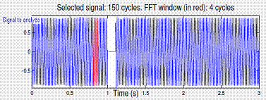
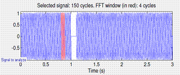
Figure 7 shows the voltage and current waveforms at the inverter end under steady state conditions. When a single phase to earth fault and three phase to earth fault is applied at t=1.0s with a duration of 5 cycles at the inverter end of an HVDC Light system, its active power, reactive power, voltage and current waveforms are shown in figure 8 and 9 respectively. Finally, the performance of SVPWM based vector controlled HVDC Light system can be seen in figure 10 in terms of THD.
|
|
|
Figure 6. Simulink model of SVPWM control of production of gate signals |
|
|
|
|
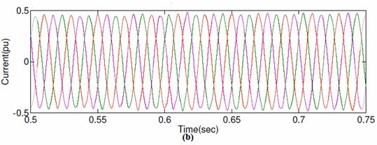
|
Figure 7. Steady state waveforms at the inverter end of SVPWM based vector controlled HVDC Light system (a) Voltage (b) current |
|
a) |
b) |
|
Figure 8. (a) Station 1 side (b) Station 2 side Waveforms of SVPWM based vector controlled HVDC Light system for a single phase to earth fault at t=1.0s at the inverter end |
|
|
a) |
b) |
|
Figure 9. (a) Station 1 side (b) Station 2 side Waveforms of SVPWM based vector controlled HVDC Light system for a three phase fault at t=1.0s at the inverter end |
|
|
a) |
|
b) |
|
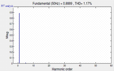
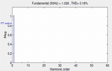
Figure 10. Output voltage and THD at the inverter end of an HVDC Light system with (a) SPWM control (b) SVPWM control |
Discussion
A single phase to earth fault was applied at t=1.0s during 5 cycles at converter 2 in order to examine the performance of SVPWM based vector controlled HVDC Light systems under unbalanced faults. From the simulation, it can be noted that before unbalanced fault, the active power flow is 0.4pu transmitted from station 1 to station 2, and is slightly reduced to 0.3pu during the fault. Voltage and current at both the stations contain small oscillations during this unbalanced fault.
Similarly, for a three phase to earth fault, ac voltage at station 2 side is decreased to 0.1pu during the fault and recovers quickly to steady state after clearing the fault. The transmitted power flow is also reduced to a very low value during the fault and recovers to steady state. On the other hand, the phase currents at station 2 reached to its maximum transient value is about 1.5pu during the fault, but the phase currents at station 1 side reduced to low values to reduce the power flow.
Finally, in figure 10 (a) and (b) it is shown that at the inverter end of SVPWM based vector controlled HVDC Light system, fundamental voltage component is 1.028pu, which is almost 15% more than SPWM controlled HVDC Light system, and THD of 0.18% with minimum power fluctuations.
Conclusion
A SVPWM based vector controlled HVDC Light transmission system, operated under steady state, balanced and unbalanced fault conditions have been simulated in this paper. Simulation results have shown that during a single phase to earth fault power can be transmitted except a small reduction during the fault. Moreover, the output voltage of the station 2 in the SVPWM based vector controlled HVDC Light system is almost 15% more than that of SPWM control, and less THD. Hence, in all cases it is evident that proposed system gives a fast and better performance in order to provide convenient, cost-effective and reliable energy to customers.
References
1. Acha E., Agelidis V.G., Anaya-Lara O., Miller T.J.E., Power Electronic Control in Electrical Systems, 1st ed. Oxford, U.K, Newnes, 2002.
2. Bahrman M.P., Johnson B.K., The ABCs of HVDC transmission technologies, IEEE Power Energy Mag, Mar./Apr. 2007, 5(2), p. 32–44.
3. Asplund G., Eriksson K., Svensson K., HVDC Light—DC transmission based on voltage-sourced converters, ABB Rev, 1998, 1, p. 4–9.
4. Gunturi S., Schneider D., On the operation of a press pack IGBT module under short circuit conditions, IEEE Trans. On Advanced Packaging, 2006, 29(3), p. 433–440.
5. HVDC and HVDC Light (online), Available at: http://www.abb.com/hvdc (accessed 20/10/2012).
6. Abbas A., Lehn P., PWM based VSC-HVDC systems-a review, Power & Energy Society General Meeting, 2009, p. 1–9.
7. Flourentzou N., Agelidis V., Demetriades G., VSC-based HVDC power transmission systems: An overview, IEEE Trans. Power Electron., 2009, 24(3), p. 592–602.
8. Shuhui Li, Haskew T.A., Ling Xu, Control of HVDC Light System Using Conventional and Direct Current Vector Control Approaches, IEEE Trans. Power Electron., 2010, 25(12), p.3106-3118.
9. Padiyar K.R., Prabhu N., Modelling, control design and analysis of VSC based HVDC transmission systems, PowerCon, 2004, 1, p. 774–779.
10. Ajay Kumar M., Archana K.U., Srikanth N.V., HVDC Light Systems: An overview, International Review on Modelling and Simulations (IREMOS), 2012, 5(5), 1951-1959.
11. Mohamed K., Ahmed Z.S., Samir H., Karim F.M., Rabie, Performance Analysis of a Voltage Source Converter (VSC) based HVDC Transmission System under Faulted Conditions, Leonardo Journal of Sciences (LJS), 2009, Issue 15 (July-December), p. 33-46.
12. Mondal S.K., Pinto J.O.P, Bose B.K., A Neural-Network-Based Space Vector PWM Controller for a Three-Level Voltage-Fed Inverter Induction Motor Drive, IEEE Trans. on I.A., 2002, 38(3), p.660-669.