Improved Switching Performance Analysis of Space Vector Pulse Width Modulation on Field Programmable Gate Array
Nagalingam RAJESWARAN1*, Tenneti MADHU2 and Munagala SURYAKALAVATHI3
1Dept. of ECE, SNS College of Technology, Coimbatore, Tamilnadu, India.
2 Swarnandhra Inst. of Engg., and Tech., Narasapur, Andhrapradesh, India.
3 Dept.of EEE, Jawaharlal Nehru Technological University, Hyderabad, Andhrapradesh, India.
E-mails: rajeswarann@gmail.com; tennetimadhu@gmail.com; mungala12@yahoo.co.in
* Corresponding author: +91-422-2666264
Abstract
Nowadays VLSI (Very Large Scale Integration) technology is being successfully implemented by using Pulse Width Modulation (PWM) in applications like power electronics and drives. The main problems in PWM viz. harmonic distortion and switching speed are overcome by implementing the Space-Vector PWM (SVPWM) technique by using the Xilinx tool VHDL (Verilog High Speed Integrated Circuit (VHSIC) Hardware Description Language) and tested in programmable Integrated Circuits of Field Programmable Gate Array (FPGA). The results are provided along with simulation analysis in terms of hardware utilization and schematic, power report, computing time and usage of memory.
Keywords
Field Programmable Gate Array; Pulse Width Modulation; Space Vector Pulse Width Modulation; Hardware Description Language
Introduction
In many new industrial applications the usage of switching power converters especially the PWM inverter controllers have lead to improvements in power electronic systems and modern motor drives [1]. The output voltage of inverter fed to the induction motor system is mainly determined by PWM strategy. When a PWM signal is applied to the gate of a power transistor, it causes the turns ON and OFF intervals of the transistor to change from one PWM period to another [2]. The major issue with PWM is the presence of harmonics. In many industrial applications, Sinusoidal PWM (SPWM), also called Sine coded PWM, is used to control the inverter output voltage [3]. The output frequency of SPWM is 50 Hz and the design is limited to two levels of modulation index viz. 0.5 and 0.75 [4]. SPWM reaches only up to 78% of square-wave operation, but the amplitude of maximum possible voltage is 90% of square-wave in the case of SVPWM. Vmax = Vdc/2 for Sinusoidal PWM and Vmax = Vdc/√3, where, Vdc is DC-Link voltage for Space Vector PWM [5].This means that SVPWM can produce about 15% higher than SPWM in output voltage and offers great flexibility to optimize switching waveforms [6 -9].
In Figure.1, the Root Mean Square (RMS) voltage is called the effective voltage, as opposed to the peak voltage which corresponds to the maximum amplitude of the voltage variations.
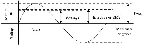
Figure 1. Sine Waveform with RMS
Total Harmonic Distortion (THD) is defined as the ratio of the rms value of the waveform not including the fundamental, to the rms fundamental magnitude [10]. When no DC is present, this can be written as,
|
THD = |
(1) |

The amplitude of the odd harmonics produced depends only upon the ratio of the dead time to the period of switching frequency. Accordingly, it has been possible to present generalized curves which allow the design engineer to estimate the amplitudes of these harmonics for any combination of fundamental and modulating frequencies [11].
PWM strategies implemented by microprocessor-based hardware and software have the advantages of flexibility, precise control and less components leading to compactness and lower cost. Space -Vector PWM provides a better technique compared to the more commonly used PWM or sinusoidal PWM (SPWM) techniques because of their easier digital realization and better DC bus utilization [12].
FPGA implementation of SVPWM provides advantages such as rapid prototyping, simpler hardware and software design, high speed computation and hence fast switching frequency [13-15]. The proposed design methodology is used for the improvement of overall performance of the SVPWM in terms of total hardware utilization in Integrated Circuits(IC).
Material and Method
Space Vector PWM in Figure 2, uses space-vectors to generate the gate signals and is implemented by averaging the time spent in adjacent switching states.
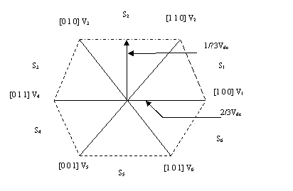
Figure 2. Space Vector Diagram
Totally six switches are used i.e, S1 to S6.The values of switching vectors are assigned in Table 1 and there are eight possible combinations of ON and OFF patterns for the three upper electronic switches from the value of 000 to 111 related with V0 to V7. Here the ON and OFF states of the lower power switches are opposite to the upper ones and are completely determined once the states of the upper power electronic switches are known. Generally, the SVPWM implementation involves sector identification, switching time calculation, switching vector determination and optimum-switching-sequence selection for the inverter voltage vectors [16].
Table 1. Illustrating Switching Vectors and Line Voltages
|
Voltage Vectors |
Switching Vectors |
Line to neutral Voltage |
Line to line voltage |
||||||
|
A |
B |
C |
Van |
Vbn |
Vcn |
Vab |
Vbc |
Vca |
|
|
V0 |
0 |
0 |
0 |
0 |
0 |
0 |
0 |
0 |
0 |
|
V1 |
1 |
0 |
0 |
2/3 |
-1/3 |
-1/3 |
1 |
0 |
-1 |
|
V2 |
1 |
1 |
0 |
1/3 |
1/3 |
-2/3 |
0 |
1 |
-1 |
|
V3 |
0 |
1 |
0 |
-1/3 |
2/3 |
-1/3 |
-1 |
1 |
0 |
|
V4 |
0 |
1 |
1 |
-2/3 |
1/3 |
1/3 |
-1 |
0 |
1 |
|
V5 |
0 |
0 |
1 |
-1/3 |
-1/3 |
2/3 |
0 |
-1 |
1 |
|
V6 |
1 |
0 |
1 |
1/3 |
-2/3 |
1/3 |
1 |
-1 |
0 |
|
V7 |
1 |
1 |
1 |
0 |
0 |
0 |
0 |
0 |
0 |
|
V0, V1 ..... V7 are the voltage vectors; A,B,C are the switching vectors of SVPWM Van,Vbn,Vcn are the Line to neutral voltage Vab,Vbc,Vca are the Line to line voltage |
|||||||||
Space vector representation of three-phase quantities xa(t), xb(t) and xc(t) with space distribution of 120o apart is given by:
|
|
(2) |
where, a = ej2p/3 = cos (2p/3) + jsin(2p/3); a2 = ej4p/3 = cos (4p/3) + jsin(4p/3); x – can be a voltage, current or flux and does not necessarily has to be sinusoidal
The waveform of SVPWM is shown in Figure.3 with the phase voltages and the total time period ‘T’. The voltages Va,Vb and Vc represent the three phase voltages of the power supply. T1, T2, T0 and T7 are calculated based on volt-second integral of vref .
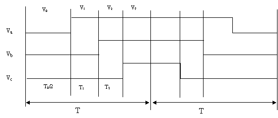
Figure 3. Waveform of SVPWM
|
|
(3) |
|
|
(4) |
|
|
(5) |
|
|
(6) |
|
|
(7) |
|
|
(8) |
Solving for T1, T2 and T0,7 gives:
|
|
(9) |
|
|
(10) |
where,
|
|
(2) |

The switching table and states are given in Table 2. To make the oscillation between the high and low states, the clock signal is applied. In Table 3, two clock signals namely clock and clk1 are used. They will be assigned as different set of offset values and make them as the rising edge. The Clock to setup on destination clock CLK1 and Clock are 10.267ns and 5.991ns respectively. Two different reset signals are used in the design. First reset signal is set as low and second reset signal rst is set high for the simulation of the assigned input.
|
Table 2. Switching table |
Table 3. Simulation parameters |
|||||||||||||||||||||||||||||||||||||||||||||||||||||||||
|
|
|||||||||||||||||||||||||||||||||||||||||||||||||||||||||
FPGA Implementation
The selected FPGA device is xc3s500e-4-pq208. The total available pin of the selected FPGA device is P208.The total allotted pins for the input and output is 23. The Input and Output (IOB) properties of the device are given in the Table 4. The static timing report and clock reports simulation outputs (screen shots) are shown in Figures 4-6. All the values are given in nanoseconds (ns). The four clock regions X0Y0, X1Y0, X0Y1 and X1Y1 are used in the design. The summary of the components used in these regions are given in Table 5.
In digital implementation, this algorithm is simplified in the hardware design (Shown in Figures 7-8). The RTL and technological view of SVPWM in FPGA are shown in Figures 9 and 10. The Number of External Input IOBs are 7, Number of External Input IBUFs are 7, Number of External Output IOBs are 16, and Number of External Bidir IOBs are 0. Overall effort level (-ol): Standard, Placer effort level (-pl): High, Placer cost table entry (-t): 1 and Router effort level (-rl): Standard. The synchronization of different modules is one of the important tasks in IC. The timing reports have clearly proved that there is an overall improvement in the performance of the design. It will reduce the complexity of the IC and make it becomes more fast.
Table 4. IOB Properties
|
IOB Name |
Type |
Direction |
IO Standard |
Drive Strength |
PIN Number |
|
CLK1 |
IBUF |
INPUT |
LVCMOS25 |
|
P184 |
|
CLK_out<0> |
IOB |
OUTPUT |
LVCMOS25 |
12 |
P112 |
|
CLK_out<1> |
IOB |
OUTPUT |
LVCMOS25 |
12 |
P116 |
|
CLK_out<2> |
IOB |
OUTPUT |
LVCMOS25 |
12 |
P115 |
|
CLK_out<3> |
IOB |
OUTPUT |
LVCMOS25 |
12 |
P109 |
|
CLK_out<4> |
IOB |
OUTPUT |
LVCMOS25 |
12 |
P119 |
|
CLK_out<5> |
IOB |
OUTPUT |
LVCMOS25 |
12 |
P120 |
|
CLK_out<6> |
IOB |
OUTPUT |
LVCMOS25 |
12 |
P113 |
|
CLK_out<7> |
IOB |
OUTPUT |
LVCMOS25 |
12 |
P123 |
|
RST |
IBUF |
INPUT |
LVCMOS25 |
|
P106 |
|
VALUE<0> |
IBUF |
INPUT |
LVCMOS25 |
|
P110 |
|
VALUE<1> |
IBUF |
INPUT |
LVCMOS25 |
|
P108 |
|
clock |
IBUF |
INPUT |
LVCMOS25 |
|
P183 |
|
enable |
IBUF |
INPUT |
LVCMOS25 |
|
P107 |
|
reset |
IBUF |
INPUT |
LVCMOS25 |
|
P130 |
|
wave_out<0> |
IOB |
OUTPUT |
LVCMOS25 |
12 |
P132 |
|
wave_out<1> |
IOB |
OUTPUT |
LVCMOS25 |
12 |
P133 |
|
wave_out<2> |
IOB |
OUTPUT |
LVCMOS25 |
12 |
P128 |
|
wave_out<3> |
IOB |
OUTPUT |
LVCMOS25 |
12 |
P129 |
|
wave_out<4> |
IOB |
OUTPUT |
LVCMOS25 |
12 |
P134 |
|
wave_out<5> |
IOB |
OUTPUT |
LVCMOS25 |
12 |
P135 |
|
wave_out<6> |
IOB |
OUTPUT |
LVCMOS25 |
12 |
P137 |
|
wave_out<7> |
IOB |
OUTPUT |
LVCMOS25 |
12 |
P140 |
|
|
|
|
Figure 4. Simulation output of Clock Clock to PAD |
Figure 5. Simulation output of Clock CLK1 to PAD |
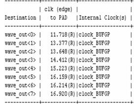
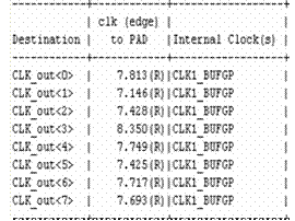
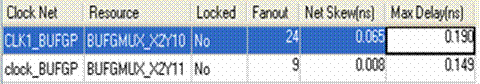
Figure 6. Simulation output of Clock Report
Table 5. Summary of Components used in the clock
|
Clock Region X1Y0 |
Module |
Used |
Available |
Percentage(%) |
|
DIFFM |
6 |
29 |
20 |
|
|
DIFFS |
7 |
29 |
24 |
|
|
IBUF |
2 |
11 |
18 |
|
|
SLICEL |
20 |
582 |
3 |
|
|
SLICEM |
20 |
582 |
4 |
|
|
Clock Region X0Y1 |
DIFFMI |
1 |
11 |
9 |
|
DIFFSI |
1 |
11 |
9 |
|
|
Clock Region X1Y1 |
BUFGMUX |
2 |
6 |
33 |
|
DIFFM |
3 |
29 |
10 |
|
|
DIFFS |
3 |
29 |
10 |
|
|
SLICEL |
23 |
582 |
3 |
|
|
SLICEM |
25 |
582 |
4 |
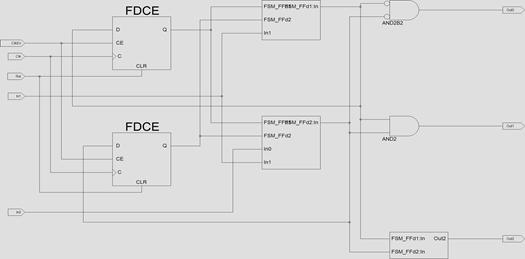
Figure 7. RTL Internal block view of SVPWM
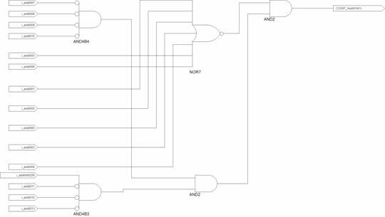
Figure 8. Gate level schematic view
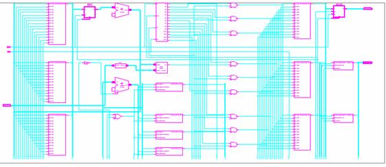
Figure 9. RTL View of SVPWM
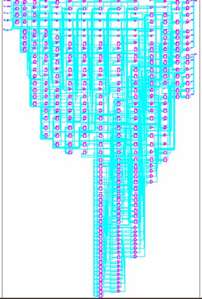
Figure 10. Technological view
Results and Discussions
The design and FPGA implementation of programmable Space Vector Pulse width Modulation (SVPWM) control circuit is presented. The Total simulation time is 11.854ns (8.042ns logic, 3.812ns route) (67.8% logic, 32.2% route), Total memory usage is 164308 kilobytes. Total REAL time to Xst completion is 6.00 secs and Total CPU time to Xst completion is 5.92 secs. The data flow schematic, shown in Figure 11, with the signals are represented as clock, reset, enable, state, next_state, table_index, clk1, rst, value wave_out. The signals clk_out, and wave_out are assigned values as height 50, offset value 5.0 and scale of 0.777. The total length is 8 bits.
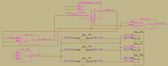
Figure 11 Data flow model of SVPWM
Once the inputs are assigned, the program runs and the outputs are displayed as a waveform. The simulated output for the SVPWM using Xilinx tool is shown in Figure 12. The timing summary is tabulated in Table 6. In Table 7, the maximum utilization of hardware is only 2-3 percentage compared with the available units. The requirement of power to produce the output is 0.081W.
Table 6. Timing Summary
|
Parameters |
Frequency |
|
Minimum period |
10.857 ns |
|
Maximum Frequency |
92.108 MHz |
|
Minimum input arrival time before clock |
6.647 ns |
|
Maximum output required time after clock |
11.854 ns |
|
Maximum combinational path delay |
No path found |
Table 7. Device Utilization Summary
|
Parameters |
Used |
Available |
Utilization |
|
Logic Utilization |
53 |
9312 |
1% |
|
Number of Slice Flip Flops |
|||
|
Number of 4 input LUTs |
153 |
9312 |
1% |
|
Logic Distribution |
96 |
4656 |
2% |
|
Number of occupied Slices |
|||
|
Number of Slices containing only related logic |
96 |
96 |
100% |
|
Number of Slices containing unrelated logic |
0 |
96 |
0% |
|
Total Number of 4 input LUTs |
185 |
9312 |
2% |
|
Number used as logic |
153 |
||
|
Number used as a route-thru |
32 |
||
|
Number of Bonded IOBs |
23 |
158 |
14% |
|
Number of BUFGMUXs |
2 |
24 |
8% |
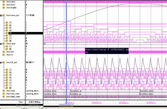
Figure 12. Switching waveform
The screen shot of power analysis report and thermal information are shown in Figure. 13 a and 13 b. The obtained ambient and junction temperature values are less. All the analysis reports have clearly proved that the SVPWM technique is efficiently programmed and implemented in IC.
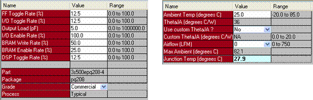
Figure 13a and 13b. Screen shot of Power Analysis and Thermal Information report
Conclusions
The performance of SVPWM improves with increased switching frequency. This technique when implemented in real time will reduce the hardware complexity and hence can be used for the testing of three phase induction motor and other power electronic devices.
References
1. Attaianese C., Nardi V., Tomasso G., A novel SVM strategy for VSI dead-time-effect reduction, IEEE Trans.on Industry Applications, 2005, 41(6), p. 1667-1674.
2. Singh M.N.B., Singh J., Improvement of Power Factor and Reduction of Harmonics in Three- Phase Induction Motor by PWM Techniques, A Comprehensive Literature Survey, Int. J. Engg. Techsci., 2011, 2(3), p. 257-269.
3. Huang S., Pham D.C., Huang K., Cheng S., Space vector PWM techniques for current and voltage source converters: A short review, 15th International Conference on, Electrical Machines and Systems (ICEMS), Sapporo, JAPAN, October 21-24, 2012, 1(6), p. 21-24.
4. Abu Bakar A., Ahmad M.Z., Abdullah F.S., Design of FPGA Based SPWM Single Phase Inverter, Proceedings of Malaysian Technical Universities Conference on Engineering and Technology, MS Garden,Malaysia, June 20-22, 2009, p. 1-5.
5. Hendawi E., Khater F., Shaltout A., Analysis, Simulation and Implementation of Space Vector Pulse Width Modulation Inverter, Proceedings of the 9th WSEAS International Conference on Application of Electrical Engineering, Penang, Malaysia, March 23-25, 2010, p. 124-131.
6. Kumar K.V., Michael P.A., John J.P., Dr. Kumar S.S., Simulation and Comparison of SPWM and SVPWM control for three phase inverter, ARPN Journal of Engineering and Applied Sciences, 2010, 5(7), p. 61-74.
7. Yumurtaci M., Ustun S.V., Nese S.V., Cimen H., Comparison of Output Current Harmonics of Voltage Source Inverter used Different PWM Control Techniques, WSEAS Trans.on power systems, 2008, 3(11), p. 695-704.
8. Erickson R.W., Maksimovic D., Fundamentals of Power Electronics, second Edition, Kluwer academic Publisher, New York, USA, 2004.
9. Sethi R., Bansal P.N., Simulation and Comparison of SPWM AND SVPWM Control for Three phase RL load, International Journal of Research in Engineering & Applied Sciences, IJREAS, 2012, 2(2), p. 1623-1636.
10. Lopez O., Alvarez J., Doval-Gandoy J., Freijedo F.D., Nogueiras A., Lago A., Penalver C.M., Comparison of the FPGA Implementation of Two Multilevel Space Vector PWM Algorithms, IEEE Trans. on Industrial Electronics, 2008, 55(4), p. 1537-1547.
11. Evans P.D., Close P.R., Harmonic distortion in PWM inverter output waveforms, Electric Power Applications, IEEE Proceedings B (Electric Power Applications), 1987, 134(4), p. 224-232.
12. Gaballah M.M., Design and Implementation of Space Vector PWM Inverter Based on a Low Cost Microcontroller, Arab J Sci Eng., Springer-Verlag, 2012, p. 1-12.
13. Rashidi B., Sabahi M., High Performance FPGA Based Digital Space Vector PWM Three Phase Voltage Source Inverter, I.J. Modern Education and Computer Science, 2013, 1, p. 62-71.
14. Koutroulis E., Dollas A., Kalaitzakis K., High-frequency pulse width modulation implementation using FPGA and CPLD ICs, Journal of Systems Architecture, Elsevier, 2006, 52, p. 332-344.
15. Tzou Y.Y., Hsu H.J., FPGA realization of space vector PWM control IC for three-phase PWM inverters, IEEE Trans. Power Electron., 1997, 12(6), p. 953-963.
16. Celanovic N., Boroyevich D., A fast space-vector modulation algorithm for multilevel three-phase converters, IEEE Trans. on Industry Applications, 2001, 37(2), p. 637-641.