Design and analysis of high gain array antenna for wireless communication applications
Sri Jaya LAKSHMI1, Habibulla KHAN2, Boddapati Taraka Phani MADHAV3
1WOS, Department of ECE, K L
University,
2Dean (SA), Department of ECE,
K L University,
3Member IEEE, Associate Professor,
Department of ECE, K L University,
E-mails: 1srijaya@kluniversity.in; 2habibulla@kluniversity.in; 3btpmadhav@kluniversity.in
Abstract
The array of antennas generally used for directing the radiated power towards a desired angular sector. Arrays can be used to synthesize a required pattern that cannot be achieved with a single element. The geometrical arrangement, number of elements, phases of the array elements and relative amplitudes depends on the angular pattern. This paper is focused on the issues related to the design and implementation of 4×1 array microstrip antenna with aperture coupled corporate feed for wireless local area network applications. Parametric analysis with change in element spacing is attempted in this work to understand the directional characteristics of the radiation pattern. Gain of more than 14 db and the efficiency more than 93% is achieved from the current design at desired frequency band.
Keywords
Antenna array; WLAN (Wireless local area network); Aperture coupling; Gain; Efficiency
Introduction
A microstrip antenna arrays is a set of two or more than two elements arranged on a single substrate material in a particular order [1]. Antenna array can be used to boost the overall gain, provide diversity reception, cancel out interference from particular direction, determines the direction of arrival of particular signal and maximizes the SNIR (Signal to Interference plus Noise ratio). Arrays can also be used for the steering operation i.e. most sensitive to particular direction. Once an array is designed to focus towards a particular direction, it will be a simple matter to steer it towards some other direction by changing the relative phases of the array elements is called the scanning. By placing proper dimensional structures in the arrays, we can design the antennas with low side lobes and good radiation characteristics. Antennas with low side lobes and back lobes can improve the directivity and the efficiency [2].
The performance of the antenna array can be increased by increasing number of elements in the array [3-4]. The drawback with increasing the number of elements [5-7] is cost, size and complexity also increases. In reality, antennas placed in close proximity to each other interact strongly. This interaction is called mutual coupling effect and it will distort the array characteristics, such as the array pattern, from those predicted based on the pattern multiplication principle. In general the effect of mutual coupling is to be considered in order to apply the pattern multiplication principle. If there is no mutual coupling effect, the excitation currents also differ by a phase difference of β and have an equal magnitude. When we consider mutual coupling into the account, the two coupled antennas can be modelled as two equivalent circuits.
The array factor AF is independent of the antenna type by assuming all of the elements are identical. Thus, isotropic radiators may be used in the derivation of the array factor to simplify the algebra. The field of an isotropic radiator located at the origin may be written as
|
|
(1) |
Here the elements of the array are uniformly spaced with a separation of distance d. Here Io is the current element located at origin. The far field of the individual array elements are
|
|
(2) |
|
|
(3) |
|
|
(4) |
|
|
(5) |
The overall array factor in the far field is
|
|
(6) |
where Eɵn is the far field factor with array elements, ‘r’ is the radius, ‘d’ is the distance between array elements, ‘k’ is the Boltzmann constant, ‘N’ is the number of elements and ‘AF’ is the array factor.
An array of antennas may be used in different ways to improve the performance of a communications engineering system [8-9]. Perhaps most important is its capability to cancel co-channel interferences. An array works on the premise that the desired signal and unwanted co-channel interferences arrive from the different directions.
The beam pattern of the array is adjusted to suit the requirements by combining signals from various antennas with appropriate weighting. Array design suitable for mobile communications is an active area of the research, and many prototypes have been built, analysed, and tested.
Microstrip array antenna with low weight and profile are suitable for numerous microwave and millimetre wave applications. Aperture coupled feeding [10-12] is used in this design to excite the array elements as shown in Figure 1.
This paper is focused on the issues related to the design and implementation of 4×1 array microstrip antenna with aperture coupled corporate feed for wireless local area network applications.
Material and method
Antenna description
Single elements of the microstrip patch array are fed by quarter wave microstrip transformer lines connected to the patch. These quarter wave transformers feeding the patch elements match the patch input impedance to impedance which is practically realizable using microstrip lines. All the four patch elements are placed in linear fashion with a perfect power diving network to match the impedance as shown in Figure 1. Each patch element consisting of the dimensions of 18X14 mm on the RT-duroid substrate material of dielectric constant 2.2 and loss tangent 0.009. The overall dimensions of the antenna are around 151X85X1.6 mm can be observed from Table 1. Aperture coupled feeding is used in this design to improve the impedance bandwidth by connecting feed lines beneath the slotted patch elements. Power diving circuit is used in the feeding network to transfer equal amount of power to all the patch elements as shown in figure
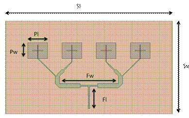
Figure 1. 4X1 Antenna array
Table 1. Array antenna dimensions
|
Parameter |
Sl |
Sw |
Pl |
Pw |
Fl |
Fw |
|
Dimensions in mm |
151 |
85 |
18 |
14 |
53 |
20 |
Algorithm and methodology
The current linear array antenna model is designed for a specific directivity and gain. The orientation is chosen along the x-axis, and element spacing and distribution taper are chosen to suite the specified objective.
Initially orientation along x, y and z are chosen in the proper way. Measurements regarding element spacing between the array elements are calculated and placed accordingly. Side-lobe levels at specified side-lobe level are estimated depending on the design equations.
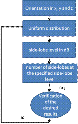
Figure 2. Proposed Algorithm
If simulated results are not meeting the desired output values then once again rearrange the element spacing with uniform distribution.
Results and discussion
The dimensions of the array antenna are calculated from the proposed algorithm and after that the design is carried out on electromagnetic tool HFSS. The complete design of the antenna array models are constructed from the HFSS simulator and the simulation results obtained from this tool are analysed. Figure 3 shows the reflection coefficient of the 4x1 microstrip array antenna model. A mismatched antenna will reflect some of the incident power back towards the transmitter and since this particular reflected wave is travelling in the opposite direction as the incident wave, there will be some points along the cable where the two waves are in phase and at other points where the waves are out of phase. A standing wave will form in the medium with this effect is called standing wave ratio. The return loss is the conventional way to characterize the input and output signal source. The proposed antenna is resonating at 5.85 GHz with bandwidth of 1.5 GHz. Impedance bandwidth of 15% is achieved from the current model.
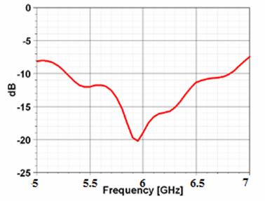
Figure 3. Reflection coefficient vs Frequency
Figure 4 shows the radiation pattern of the 4×1 antenna in E and H-planes. A radiation pattern defines the variation of the power radiated by an antenna as a function of the direction away from the antenna. This power variation as a function of the arrival angle is observed in the antenna's far field. In general, as the element spacing is increased, the main lobe beam width is decreased. However, grating lobes (maxima in directions other than the main lobe direction) are introduced when the element spacing is greater than or equal to one wavelength. If the array pattern design requires that no grating lobes be present, then the array element spacing should be chosen to be less than one wavelength. If we consider the broadside array factor as a function of the number of array elements, we find that, in general, the main beam is sharpened as the number of elements increases. E-plane is like end fire and H-plane radiation patterns is like broadside array.

Figure 4. 4×1 Antenna radiation pattern in E-Plane and H-Plane
The strength of the electric field is dependent upon how the charged object creating the field upon the distance of separation from the charged objects. Figure 5 shows the electric field distribution over the surface of the antenna at 5.85 GHz. Electric field is uniformly distributed on the patch elements with maximum intensity at the patch edges.
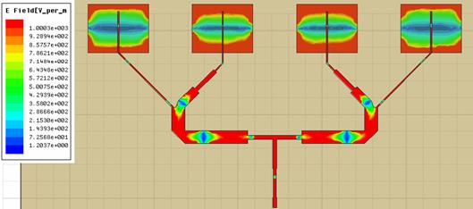
Figure 5. E-Field distribution on the surface of 4×1antenna at 5.85 GHz
The magnetic field can be visualized as magnetic field lines correspond to the density of the field lines. The total number of magnetic field lines penetrating an area is called the magnetic flux. Figure 6 shows the magnetic field distribution of the antenna at 5.85 GHz.
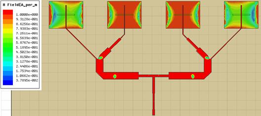
Figure 6. H-Field distribution on the surface of 4×1antenna at 5.85 GHz
Surface current distribution of the antenna is given in Figure 7. When moving away from this cross-section the components in the direction of the feed line do not cancel any more and the resulting forces increase. At larger distances, the interaction vanishes rapidly because the distance increases.
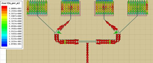
Figure 7. Current distribution on the surface of 4×1 antenna at 5.85 GHz
The element spacing in an array not only gives rise to mutual coupling, it also affects the radiation characteristics of the antenna. Figure 8 shows the antenna radiation characteristics in E and H-plane with change in the element spacing between the antenna elements. Figure 8a shows the radiation pattern in E-plane with element spacing of 0.3 to 0.5 and Figure 8b shows the radiation pattern in E-plane for element spacing from 0.6 to 0.7.
The single patch can be seen as a resonant cavity with radiating slots at each end of the patch. The fringing fields act to extend the effective length of the patch, with the result that the length of the half-wave patch is less than a half wavelength in the dielectric medium. Although simple array theory does not take mutual coupling effects into account, which may be significant for microstrip patches, it may be used to obtain a first order approximation of the resulting array pattern.
The total field of the array is determined by the vector addition of the fields radiated by the individual elements, assuming that the current in each element is the same as that of the isolated element. Figure 8 shows the radiation pattern of the array antenna in the H-plane with change in element spacing from 0.3 to 0.7. While increasing element spacing between the elements the beam becomes narrow and more directive towards particular direction as shown. It was observed that the losses associated with mutual coupling also decreased and gain factor is increased from this study.
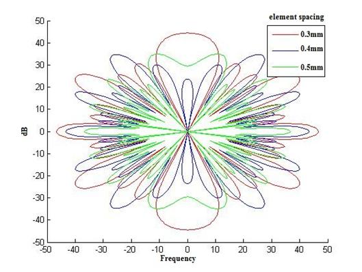
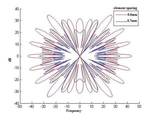
Figure 8a. Radiation pattern of the array antenna in the E-plane with change in element spacing
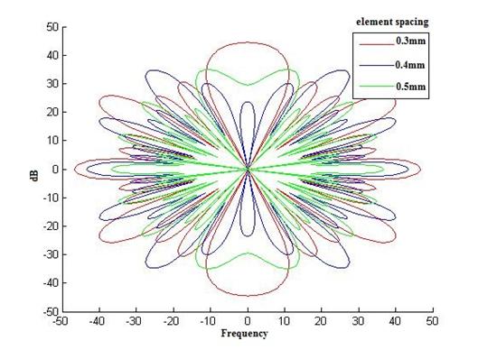

Figure 8b. Radiation pattern of the array antenna in the H-plane with change in element spacing
Table 2. 4×1 Antenna parameters
|
S. No |
Parameter |
Value |
Units |
|
1 |
Peak Directivity |
15.331 |
dB |
|
2 |
Peak gain |
14.346 |
dB |
|
3 |
Peak realized gain |
13.349 |
dB |
|
4 |
Radiated power |
0.87075 |
W |
|
5 |
Accepted Power |
0.9305 |
W |
|
6 |
Incident power |
1 |
W |
|
7 |
Radiation Efficiency |
93% |
- |
Table 2 shows the array antenna parameters at the resonating frequency. It is been observed that the antenna array is showing more than 15 dB in directivity and 14 dB in gain at resonant frequency with good radiation efficiency. The main purpose of this antenna design is to increase the gain with good radiation characteristics. The proposed model is showing excellent high gain with maximum directivity of more than 15 dB in the desired direction.
Conclusions
The proposed model is showing excellent gain and radiation characteristics at the desired frequency of operation. For proper operation the element spacing should kept between 0.5 λ0 and λ0. If the element spacing is lower than 0.5λ0, the mutual coupling between the elements becomes significant, which will increase the energy loss and make impedance matching difficult. Hence the element spacing should be greater than 0.5 λ0, however there should not be greater than λ0, otherwise the high level side lobe in the radiation pattern will occur.
Further it was observed that the parametric analysis for radiation characteristics with change in element spacing between the patches for better understanding of the radiation behaviour of the array antenna. Radiation efficiency more than 93% with maximum directivity of more than 15 dB is attained from the current design. A better way to tune the input resistance is to use an aperture coupled feed, instead of the edge feed for the patches. The overall input impedance is controlled sufficiently by adjusting the width of the input matching section of the feed network. The proposed model can be applicable for the WLAN applications, where high gain is needed with optimum power utilization.
Acknowledgements
Authors would like to express their thanks to the department of ECE and management of K L University for providing facilities at K L University to carry out this research work. Sri Jaya Lakshmi likes to express her deep gratitude towards the support from DST through women scientist scheme SR/WOS-A/ET-75/2011.
References
1. Habibulla K., Madhav B. T. P., Mallikarjun K., Bhaskar K., Sri Harsha N., Muralidhar N., Uniplanar Wideband/Narrow Band Antenna for Wlan Applications, World Applied Sciences Journal, 2014, 32(8), p. 1703-1709.
2. Madhav B. T. P., Kotamraju S. K., Manikanta P., Narendra K., Kishore M. R., Kiran G., Tapered Step CPW-Fed Antenna for Wideband Applications, ARPN Journal of Engineering and Applied Sciences, 2014, 9(10), p. 1967-1973.
3. James J., Hall P., Handbook of microstrip antennas, IEE Electron. Waves Series, 28, 1988.
4.
Pozar D., Schaubert
D., Microstrip Antennas: The Analysis and
Design of Microstrip Antennas and Arrays.
5. Madhav B. T. P., Pisipati V. G. K. M., Habibulla K., Prasad V. G. N. S., Praveen Kumar K., Bhavani K. V. L., Datta Prasad P. V., Microstrip 2×2 Square Patch Array Antenna on K15 Liquid Crystal Substrate, International Journal of Applied Engineering Research, 2011, 6(9), p. 1099-1104.
6. Madhav B. T. P., Sowjanya J., Swathi V., Tanmayee P., Circular Array Antenna Synthesis based on Element Spacing, International Journal of Applied Engineering Research, 2014, 9(20), p. 6959-6965.
7. Ramkiran D. S., Madhav B. T. P., Nimmagadda H., Sree Ramya R., Vindhya K. M., Abhishek S. P., Design and analysis of microstrip slot array antenna configuration for bandwidth enhancement, Leonardo Electronic Journal of Practices and Technologies, 2014, 25, p. 72-83.
8. Chiu C. W., Chi Y. J., Deng S. M., An internal multiband antenna for WLAN and WWAN applications., Microwave Opt. Technol. Lett., 2009, 51, p. 1803-1807.
9. Habibulla K., Madhav B. T. P., Mallikarjun K., Bhaskar K., Sri Harsha N., Muralidhar N., Uniplanar Wideband/Narrow Band Antenna for Wlan Applications., World Applied Sciences Journal, 2014, 32(8), p. 1703-1709.
10. Sullivan P. L., Schaubert D., Analysis of an Aperture-Coupled Microstrip Antenna., IEEE Transactions on Antenna and Propagation, 1986, 34(8), p. 977-984.
11. Pozar D. M., Microstrip Antenna Aperture-Coupled to a Microstrip line., Electronics Letters, 1985, 21(2), p. 49-50.
12. Vinay Balusa, Pavan Kumar V. S. K., Madhav B. T. P., Aperture Coupled Feed Circularly Polarized Antenna, SPACES-2015, 2015, pp 240-244.