Novel compact asymmetrical fractal aperture Notch band antenna
Duvuri Sri RAMKIRAN1, Boddapati Taraka Phani MADHAV1,*, Annam Manikanta PRASANTH1, Naga Sri HARSHA1, Vishnu VARDHAN1, Karimikonda AVINASH1, Maddipati Nava CHAITANYA1, Usirika Sharmila NAGASAI2
1 Department of ECE, K L University, AP, India
2 Sri Vasavi Institute of Engineering and Technology, Nandamuru
E-mails: ramkiran@kluniversity.in; *btpmadhav@kluniversity.in; annammanikanta@gmail.com; nagasriharsha@gmail.com; vishnuvardhan@gmail.com; karimikondaavinash@gmail.com; nagachaitanya@gmail.com; sharmilanagasai@gmail.com
* Corresponding author, phone: +91-9908243452
Abstract
A compact novel fractal aperture co-planar waveguide fed monopole antenna for multiband applications is proposed in this paper. The structure is asymmetric along the principle axis and seems to be like amoeba shape of radiating element. A band notch characteristic also achieved through this design for communication band applications. The antenna parameters were investigated to fully understand the behaviour and later for the optimisation process. The simulated results through HFSS tool are giving satisfactory results to notch particular band of frequencies and which is giving motivation for the fabrication of the proposed model. All the antenna parameters including S parameters and radiation patterns and current distributions are studied through simulation and experimental validation is done through the proto type modelling on FR4 substrate. Except the Notch band, the proposed antenna model giving excellent radiation characteristics with VSWR less than 2. The prototyped antenna model is occupying a compact size of 18×14×1.6 mm on FR4 dielectric substrate material with dielectric constant 4.4.
Keywords
Compact; Fractal; Asymmetrical fractal; Amoeba shape; VSWR; Notch band; Coplanar waveguide
Introduction
Multiband antennas are gaining their applications in the mobile communication fields with their compact nature [1-2]. High performance, compact size and low cost often meet their requirements for the modern microwave communication systems with their numerous advantages and applications antennas with different configurations like fractals, EBG structures and defected ground structures are been used to enhance the antenna parameters with multiband characteristics [3-8]. Miniature and low profile antennas in these categories have undesirable intrinsic attributes such as narrow band width and inefficient radiation characteristics resulting from reducing the antennas dimensions smaller than a quarter wave length at operating frequency [9-10]. It has been demonstrated that fractal geometries, which are based on space filling characteristics and self-similarity attributes, can be used to improve performance of the antenna. Also fractal based antennas can effectively coupled energy to free space. In addition, different feeding methodologies can be applied on fractal antennas without decreasing their performance for example micro strip line feed and coplanar wave line feeding methods [11-12].
Electromagnetic band gap structures are widely used to reject certain frequency band, popularly known as photonic band gap structures. However it is difficult to use an EBG structure for the design of the microwave or millimetre wave components due to the difficulties of modelling [13]. There are so many design parameters that effect on the band gap property such as number of lattice, lattice shapes, lattice spacing and relative volume fraction. Another problem is caused by the radiation from the periodic etched defects in order to minimize problems associated with EBG structures can be addressed and reduce by using special defected ground structures [14]. The defected ground structures is one of the most interesting areas of research in microwave integrated circuits with their advantages like suppression of harmonics and making compact physical dimensions of the circuit.
In this article it is designed a compact asymmetrical fractal antenna with defected ground structures to improve the performance with multiband characteristics in the operation. The fractal structure seems to be like amoeba shape and the defected ground structures are used on the ground plane to improve the wide band characteristics at multibands with notching for certain frequency bands. The detailed description regarding antenna dimensional characteristics and the corresponding parameters results are discussed in the subsequent sections.
Material and method
The complete configuration and parameters of the coplanar wave guide fed asymmetric fractal antenna with different iterations are shown in Figure 1. The structure consisting of Fractal shaped tree like monopole with defected ground on the same side of the substrate. The antenna is printed on commercial substrate material FR4 with dielectric constant 4.4 and los tangent 0.24. The overall dimension of the antenna is around 18 X 14 X 1.6mm. The proposed coplanar wave guide fed asymmetric fractal antenna consists of fractal patch with an array of fractal unit cells connected like branches to a tree.
|
a. |
b. |
|
c. |
d. |
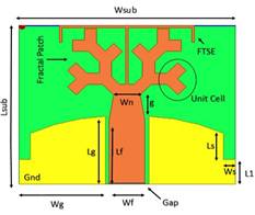
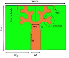
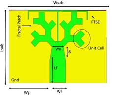
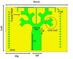
Figure 1. Notch Band Antenna Iterations
The antenna’s rectangular ground plane is etched on the same side of the substrate for a particular model and ground plane is etched with radiating element shaped slot in another model and defected ground structure with periodic holes on another model is designed and discussed in these configurations. To achieve band notch property for certain frequency bands a special type of structures on the ground planes are experimented in this work.
Table 1. Antenna parameters
|
S.No |
Parameter |
Dimensions (mm) |
|
1 |
Wsub |
18 |
|
2 |
Lsub |
14 |
|
3 |
Wf |
3 |
|
4 |
Lf |
5.5 |
|
5 |
Gap |
0.3 |
|
6 |
Wn |
2.2 |
|
7 |
g |
1.79 |
|
8 |
Wg |
7.2 |
|
9 |
Lg |
6 |
|
10 |
L1 |
2.2 |
|
11 |
Ws |
1 |
|
12 |
Ls |
2.3 |
|
13 |
Lst1 |
5.1 |
|
14 |
Lst2 |
1.5 |
|
15 |
Wst1 |
0.2 |
|
16 |
Wst2 |
5.5 |
The antenna dimensions were optimized through parametric analysis using electromagnetic tool HFSS and the final dimensional characteristics are presented in table 1.
Methodology:
1. Initially by using mathematical formulation, the dimensional characteristics of the antenna are calculated.
2. Antenna simulation is done using FEM based HFSS tool and after that optimization is done using parametric analysis.
3. Prototyped model is fabricated on FR4 substrate and tested using ZNB 20 VNA for S-parameters and Radiation characteristics. A good agreement between simulated and measured results are analyzed and presented in this work.
Results and discussion
The antenna S - parameters will give a first sight regarding its operating frequencies, impedance and band width. Figure 2 shows the S11 parameter of the antenna models with different iterations. Ground plane and radiating element are placed on single side with notch in the ground resulting dual band characteristics with resonant frequencies at 5GHz and 10GHz respectively. At 5GHz resonating frequency antenna is giving an impedance band width of 40% and at 10GHz it is giving an impedance band width of 35%. Radiating element is taken on front side with full ground on another side resulting quad band characteristics at higher frequencies between 15-30GHZ. When defected ground structure is taken on the ground plane with the same shape of the radiating element then the antenna is resonating at triple band with wide band width at the highest resonating frequency of 28GHz. At this resonant frequency antenna is showing a band width of 4GHZ with impedance band width of 14%. When defected ground structure with photonic band gap periodic design is taken on the ground plane the antenna is resonating at penta-band which covers different frequency bands between 12-30GHz.
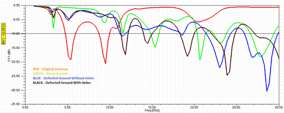
Figure 2. Return loss
The voltage standing wave ratio of all the iterations is shown in Figure 3 which also indicating the same resonating frequency parameters like return loss curve. All these iterations are maintaining a 2:1 ratio of VSWR at the corresponding resonant frequency.
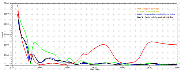
Figure 3. VSWR Plot
The radiation patterns of the antenna iterations are presented in figure 4-7.
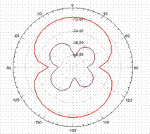
Figure 4. Antenna radiation pattern for Iteration 1
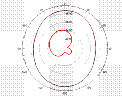
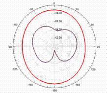
Figure 5. Antenna radiation pattern for Iteration 2
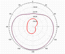
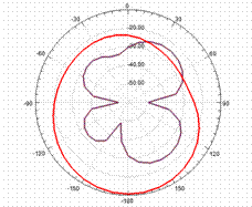
Figure 6. Antenna radiation pattern for Iteration 3
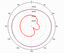
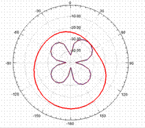
Figure 7. Antenna radiation pattern for Iteration 4
Figure 4 shows E and H plane radiation characteristics of the base model at 10 GHZ. A low cross polarization of less than -32db can be observed from H-plane characteristics of the base model. An omni directional radiation pattern also can be observed in co-polarization for H-plane. The E-plane radiation characteristics are seems to be directive with nulling at 90 degrees and 270 degrees respectively. Figure 5 shows the radiation characteristics of the second model with quasi omni directional co-polarization and low cross polarisation less than -24db. Figure 6 and 7 also show the radiation characteristics for antenna model 3&4. These models are giving directive radiation patterns in most of the cases instead of omni or quasi omni directional radiation patterns.
The complete behaviour of the antenna with respect to the mode of propagations can be analysed through current distribution characteristics results (Figure 8-11).
|
|
|
|
Figure 8. Current distribution for iteration 1 |
Figure 9. Current distribution for iteration 2 |
|
|
|
|
|
|
|
Figure 10. Current distribution for iteration 3 |
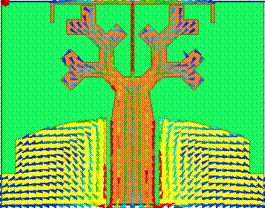
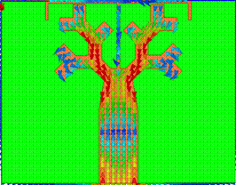
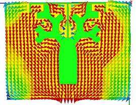
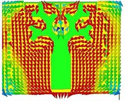
Figure 8 shows the current distribution plot of antenna1 at 10 GHz. The maximum current density is focused at the edges of fed line and near by ground plane as shown in the figure. Other than at the position nearer to fed line, the ground plane current distribution is showing low density on its surface. The branch like radiating elements connected to the tree structure also showing low current density with uni-directional flow towards feed line. Figure 9 shows the current distribution over the monopole antenna of model 2. On the feed line current elements are moving in opposite direction and meeting at the centre of feed line which results cancellation of lower operating band frequencies. Most of the current distribution with maximum intensity is focused on the branches connected to the tree shaped radiating element structure.
Figure 12 shows the peak directivity of the antenna models at their corresponding resonant frequencies.
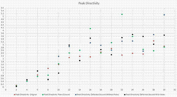
Figure 12. Frequency Vs Directivity
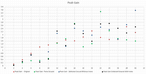
Figure 13. Frequency Vs gain
A maximum directivity of 5dB is attained for model 2 at 22 GHz resonant frequency. An average directivity of 2.4 dB is attained for model 4. Figure 13 shows frequency vs gain plot for antenna models. A maximum gain of 3.6 dB is attained for the model defected ground without holes. An average gain of 2db is attained for defected ground with PBG structured model. Figure 14 shows the prototyped antenna on FR4 substrate with thickness 1.5mm.
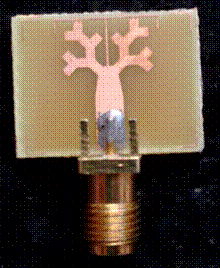
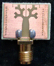
Figure 14. Prototyped antenna on FR4 substrate, (a) Top View, (b) Bottom view
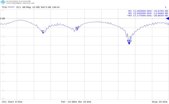
Figure 15. Measured S11 of antenna on ZNB 20 VNA
The bottom view of the antenna with slotted portion similar to the radiating element and rectangular slots on either side can be observed. An SMA connector is connected at 50 ohms impedance point on the feed line can be observed in the Figure 14.
Figure 15 shows the measured reflection coefficient of the antenna with the help of R&S ZNV 20 Vector Network Analyzer. The results obtained from the VNA are similar to that of simulation results obtained from the HFFS Simulation tool.
Conclusions
A compact Fractal Aperture Notch Band Antenna is designed and prototyped in this work. The proposed antenna is working at different frequency bands and notching certain frequency bands in the communication systems frequency range. A maximum directivity of 5 dB and maximum gain of 3.6 dB is attained from the current design.
Antenna is showing excellent radiation characteristics with rejection of particular frequency bands with the help of defected ground structure on the bottom surface gives motivation to use the proposed antenna in the desired communication band of operations. The prototyped antenna is measured with ZNB 20 vector network analyzer and obtained results on the instrument are in good agreement with the simulation results obtained from the high frequency structure simulation tool.
Acknowledgements
Authors would like to express their gratitude towards the department of ECE and management of K L University for their support and encouragement during this work. Further Madhav likes to express his gratitude to DST through FIST grant SR/FST/ETI-316/2012.
References
1. Schantz H. G., Wolenec G., Myszka E., Frequency notched UWB antennas, Proc. IEEE Conf. Ultra Wideband Syst. Technol., 2003, p. 214-218.
2. Madhav B. T. P., Chhatkuli S., Manikantaprasanth A., Bhargav Y., Venkata Sai U. D. N., Feeraz S., Measurement of dimensional characteristics of microstrip antenna based on mathematical formulation, International Journal of Applied Engineering Research, 2014, 9(9), p. 1063-1074.
3. Madhav B. T. P., Prasanth A. M., Prasanth S., Krishna B. M. S., Manikantha D., NagaSai U. S., Analysis of defected ground structure Notched Monopole antenna, ARPN Journal of Engineering and Applied Sciences, 2015, 10(2), p. 747-752.
4. Madhav B. T. P., Vaishnavi G., Manichandana V., Reddy C. H., Teja S. R., Sesi Kumar J., Compact Sierpinski carpet antenna on destructive ground plane, International Journal of Applied Engineering Research, 2013, 8(4), p. 343-352.
5. Lin Y. C., Hung K. J., Compact ultra-wideband rectangular aperture antenna and band-notched designs, IEEE Trans. Antennas Propag., 2006, 54(11), p. 3075-3081.
6. Madhav B. T. P., Yedla K. N., Kumar G. S., Rahul K. V. V., Fractal aperture EBG ground structured dual band planar slot antenna, International Journal of Applied Engineering Research, 2014, 9(5), p. 515-524.
7. Madhav B. T. P., Pisipati V. G. K. M., Khan H., Ujwala D., Fractal shaped Sierpinski on EBG structured ground plane, Leonardo Electronic Journal of Practices and Technologies, 2014, 25, p. 26-35.
8. Madhav B. T. P., Gogineni J., Appana H., Chennam J. P., Thota D. S. S., Kotte P., Analysis of compact coplanar waveguide fed slot antenna with EBG structure, Spaces, 2015, p. 219-225.
9. Madhav B. T. P., Kumar K. V. V., Manjusha A. V., Chowdary P. R. B., Sneha L., Kantham P. R., Analysis of CPW fed step serrated ultra wide band antenna on rogers RT/Duroid substrates, International Journal of Applied Engineering Research, 2014, 9(1), p. 53-58.
10. Madhav B. T. P., Khan H., Ujwala D., Sankar Y. B., Kandepi M., Siva Nagendra Reddy A., Nagajyothi D., CPW Fed Serrated Antenna Performance Based on Substrate Permittivity, International Journal of Applied Engineering Research, 2013, 8(12), p. 1349-1354.
11. Sze J. Y., Shiu J. Y., Design of band-notched ultrawideband square aperture antenna with a hat-shaped back-patch, IEEE Trans. Antennas Propag., 2008, 56(10), p. 3311-3314.
12. Madhav B. T. P., Pisipati V. G. K. M., Khan H., Prasad V. G. N. S., Praveen Kumar K., Bhavani K. V. L, Ravi Kumar M., Liquid crystal bow-tie microstrip antenna for wireless communication applications, Journal of Engineering Science and Technology, 2011, 4(2), p 131-134.
13. Peng L., Ruan C. L., UWB band-notched monopole antenna design using electromagnetic-bandgap structures, IEEE Trans. Microw. Theory Tech., 2011, 59(4), p. 1074-1081.
14. Madhav B. T. P., Mohan Reddy S. S., Ravindranath Chowdary J., Vinod Babu V., Satya Parthiva S. S., Kalyana Saravana S., Analysis of dual feed asymmetric antenna, International Journal of Applied Engineering Research, 2013, 8(4), p. 361-367.