Ultra low voltage and low power Static Random Access Memory design using average 6.5T technique
Nagalingam RAJESWARAN1,*, Tenneti MADHU2, Bini JOY1, and Ruth Anita SHIRLEY1
1Department of ECE,SNS College of Technology, Coimbatore, Tamilnadu, India
2 Swarnandhra Inst.of Eng. and Tech., Narasapur,Andhrapradesh,India
E-mails: rajeswarann@gmail.com; tennetimadhu@gmail.com; bini251990@gmail.com; ruthshirley06@gmail.com
* Corresponding author: +91-422-2666264
Abstract
Power Stringent Static Random Access Memory (SRAM) design is very much essential in embedded systems such as biomedical implants, automotive electronics and energy harvesting devices in which battery life, input power and execution delay are of main concern. With reduced supply voltage, SRAM cell design will go through severe stability issues. In this paper, we present a highly stable average nT SRAM cell for ultra-low power in 125nm technology. The distinct difference between the proposed technique and other conventional methods is about the data independent leakage in the read bit line which is achieved by newly introduced block mask transistors. An average 6.5T SRAM and average 8T SRAM are designed and compared with 6T SRAM, 8T SRAM, 9T SRAM, 10T SRAM and 14T SRAM cells. The result indicates that there is an appreciable decrease in power consumption and delay.
Keywords
Low power 1; Delay; Memory; Average nT; 125nm technology
Introduction
Static Random Access Memory (SRAM) cells are widely used as memory devices in computer systems due to their low power consumption [1]. A basic SRAM cell is made up of six transistors. This storage cell has two stable states which are used to denote on and off. Two additional access transistors provide access to a storage cell during read and write operations. In addition to such six transistors SRAM, other kinds of SRAM chips that use more transistors per bit are also available [2].
The Complementary Metal Oxide Semiconductor (CMOS) SRAM cell is very less power consuming and has less read and write time. Stability can be improved by maintaining high cell ratios. It can be seen that increased memory capacity increases the bit line parasitic capacitance which in turn slows down voltage sensing and make bit-line voltage swings energy expensive. This result shows the slower and more energy hungry memories [3]. Reverse short channel effect is utilized in SRAM cell design which improves cell write margin and read performance without using additional circuits. Marginal Bitline Leakage Compensation (MBLC) scheme compensates for the bit line leakage current which becomes comparable to a read current at sub threshold supply voltages [4]. Data stability of SRAM cells has become an important issue with the scaling of CMOS technology. The standby 9T SRAM cells are placed into a cut off sleep mode, as a result reduces the leakage power consumption. The reduction of leakage power and read stability enhancement provided with the new circuit technique are also verified under process parameter variations [5]. Due to reduction in SRAM operating voltage, cell stability degradation occurs with the increase in process variation and process scaling. Hence 10T SRAM cell reducing the total leakage power consumption as well as maintaining the performance of SRAM cells were designed [6].
The main aim of this paper is to reduce the power consumption and delay of the average nT technique SRAM design. The proposed design of an average 6.5T SRAM compared with 6T SRAM, 8T SRAM, 9T SRAM, 10T SRAM and 14T SRAM cells. The obtained result indicates that there is an appreciable decrease in power consumption and delay.
Material and method
The block diagram of 128 KB memory is shown in Figure 1. It consists of 128 columns and 256 rows. Average 8T, Address decoder, sense amplifier and bit line multiplier are the various blocks of 128KB memory.
In Figure 1 is given the design of 128 Kb memories:
128kb = 128000 = 217 = 210 x 27= 1, 31,072 = 1024x128
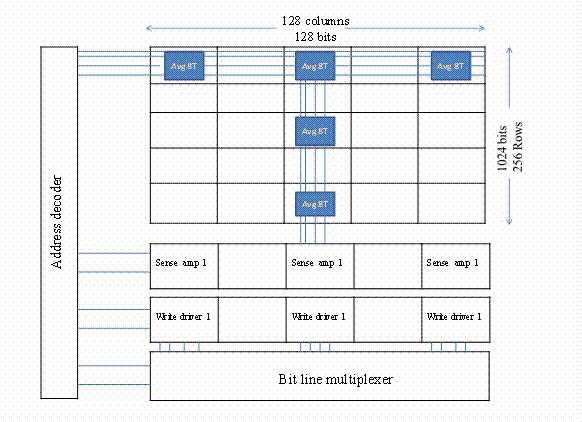
Figure 1. Block diagram of 128kb memory
Each Average 8-T block can hold 4 bits. It has 128 columns and 256 rows. The proposed architecture is flexible in providing blocks of different number of bits ranging from 1 to 16 bits per block.
Sense amplifier
Sense amplifier is the only analogue circuit in a computer's memory and is a major part of read circuitry used for reading data from the memory. Numerous functions that influence the performance, reliability and functionality of the memory are dedicated to the sense amplifiers. Amplification is essential for memories, allowing a reduced voltage swing on the bit lines thereby reducing the power dissipation and delay. Hence, the sense amplifier senses the bit-line for low power signals and amplifies it to recognizable logic levels so that the data can be transferred properly by logic outside the memory. Hundreds of sense amplifiers are present on a modern memory chip.
Address decoders
Address decoders (Row and Column decoders) are essential for a random address based access memories. Designing these decoders has a substantial impact on the power consumption and delay of the memory. The function of row decoder is to select one row out of 2M input multiplexers. The last action to be performed in the read sequence is the column decoding. The propagation delay induced by the decoder is of prime importance as it affects both write and read access times. A mismatch between the cell dimensions of decoders and the core leads to a noticeable wiring overhead with its associated delay and power consumption.
Bit- Line Multiplexer
An SRAM multiplexing circuit consists of a local multiplexer and a global multiplexer. Local multiplexer's and their respective memory banks are connected to each other. The global multiplexer has a number of inputs, each of which is coupled to a corresponding output of the local multiplexers. In response to a decoded address in a read operation, local multiplexer's input is forwarded to a corresponding input of the global multiplexer. In the same manner, the global multiplexer forwards the input signals to a data out port through a buffer.
6T SRAM Cell
The generic SRAM cell is shown in Figure 2, and turns out to be virtually identical to that of a static SR latch. It requires six transistors per bit. Access to the cell is enabled by the word line, and controls two pass transistors M5 and M6. It has two bit lines transferring both the stored signal and its inverse. SRAM cell should be sized as small as possible to achieve high memory densities. SRAM cell operates in three modes: Standby mode, Read and Write modes. During standby mode the Write Line (WL) is grounded and the cell is able to hold the data as long as it is powered. The values stored at QB and Q, during read operation are transferred to the bit lines by using M1-M5 to discharge Bit Line Bar (BLB) and leaving Bit Line (BL) at its pre-charged value.
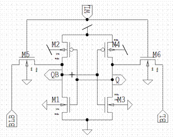
Figure 2. Schematic of 6T SRAM cell
The output for 6T SRAM cell is shown in Figure 3. Here BL, BLB, WL are the inputs and Q and QB are the output wave. As the difference between the two builds up, the sense amplifier is activated to accelerate the reading process. The drawback of 6T SRAM cell is the stability problem which arises during Read and Write operation where the cell is most vulnerable towards noise [7].
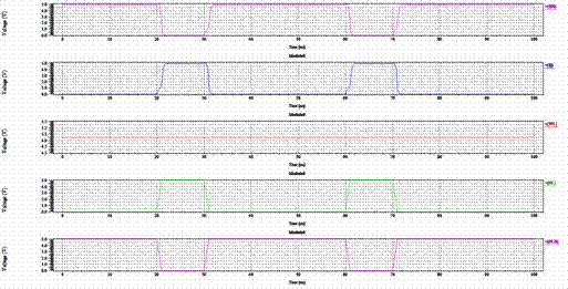
Figure 3. Output Waveform of 6T SRAM Cell
8T SRAM Cell
The 8T SRAM cell is as shown in Figure 4. The stability problem which occurs during read operation in 6T is overcome by an 8T cell by using separate Read/Write bit-lines and write signal lines [8]. Write access and read access to the cell occurs separately through their respective write access transistors from the write bit-lines, Write Bit Line (WBL) and Write Bit Line Bar (WBLB) and through the read access transistors controlled by the Read Word Line (RWL). The Read Bit Line (RBL) is pre-charged prior to the read access.
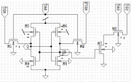
Figure 4. Schematic of 8T SRAM cell
The output for 8T SRAM cell is shown in Figure 5. Here WBL, WBLB, WL are the inputs and Q and QB are the output wave. But the drawback is that the bit line leakage for read is greater for the 8T SRAM. When the column for Read (RBL) is not accessed, the leakage current through M8 may cause severe voltage drop at the read bit line, leading to large Power dissipation [9-10].
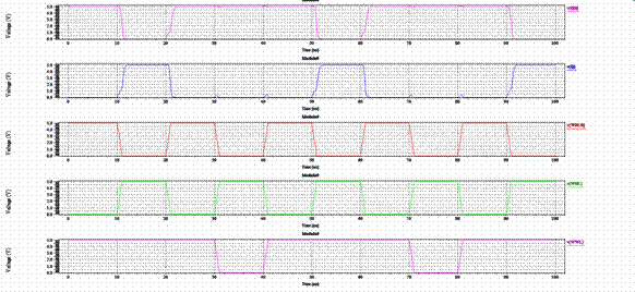
Figure 5. Output Waveform of 8T SRAM Cell
Results and discussion
9T SRAM Cell
A 9T SRAM structure is designed to overcome the drawback of 8T. Figure 6 shows the structure of 9T SRAM that is proposed to decrease the bit-line leakage as well as the power consumption. Transistors M1 to M6 have the same configuration as that of the 8T cell. Bit-line leakage problem for the 8T cell has been noticed on the read bit-line. Hence, during the read operation, it is possible that data is modified. In other words, the bit-line drops to a lower level despite being kept high because of bit-leakage due to other un-accessed cells. This imposes a low-density application limitation on the 8T cell. Between M8 and M7, an additional NMOS transistor M9 is introduced in order to decrease the bit-line leakage by stack effect [11].
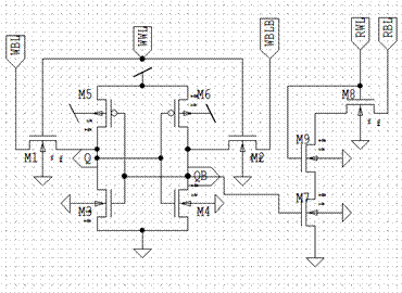
Figure 6. Schematic of 9T SRAM Cell
In Figure 7, is the output for 9T SRAM cell. Here WBL, WBLB, WL are the inputs and Q and QB are the output wave. An appreciable reduction in bit-line leakage makes this SRAM suitable for high-density SRAM designs by including more number of SRAM cells per bit-line. The size of SRAM cell should be as small as possible.
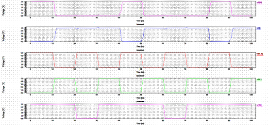
Figure 7. Output Waveform of 9T SRAM Cell
10T SRAM Cell
The Structure of 10T SRAM cell is shown in the Figure 8. During read mode, WL is enabled and ground is forced to 0 V. By disabling WWL storage nodes ‘Q’ and ‘QB’ are decoupled during read access from the bit line [12-13]. Thus the read stability is appreciably improved in 10T cell. Based on the value stored in the cell, and by enabling the word line discharging of one of the bit lines takes place.
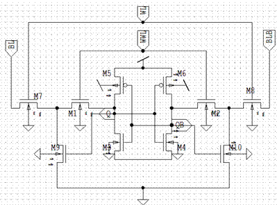
Figure 8. Schematic of 10T SRAM cell
In Figure 9, is the output for 10T SRAM cell. Here BL, BLB, WWL are the inputs and Q and QB are the output wave. The position of BL and BLB can be interchanged because the read value is same as the inverted signal of the data in the cell. During write mode, both the word lines are enabled and thus the data is written from the bit-lines to the cell [14].
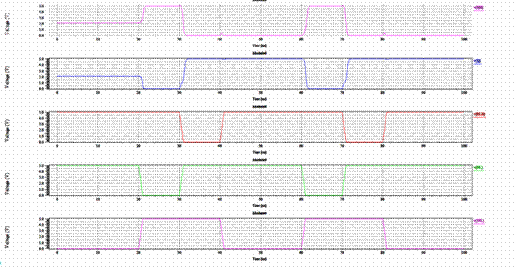
Figure 9.Output Waveform of 10T SRAM Cell
14T SRAM Cell
The Structure of 14T SRAM is shown in Figure 10. Here the storage nodes are fully separated from the read/write bit lines thereby improving the stability to a great extent.
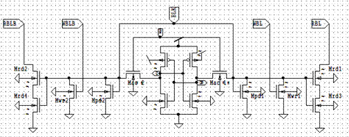
Figure 10. Schematic of 14T SRAM cell
In Figure 11, is the output for 14T SRAM cell. Here WBL, WBLB, WL are the inputs and Q and QB are the output wave. Performance of the cell is also improved by decoupling the read and write bit-lines from one another.
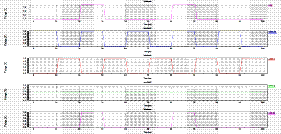
Figure 11. Output waveform of 14T SRAM Cell
Average 8T SRAM Cell
The basic architecture of the proposed write/read-decoupled SRAM block is illustrated in Figure 12. The number of transistors in each block depends on the number of bits stored in the block.
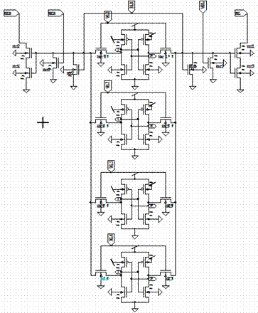
Figure 12. Schematic of Average 8T SRAM Cell
The average-8T block is capable of holding four bits through four back-to-back connected inverters. In Figure 13 is the output for Average 8T SRAM cell. Here WBL, WBLB, WL are the inputs and Q and QB are the output wave. The storage nodes are connected to the local bit-lines (LBL and LBLB) via access transistors Mac1–8. These local bit-lines are decoupled from the write bit-lines (WBL and WBLB) via the write transistors Mwr1–2 during a write operation and from the global read bit-lines (RBL and RBLB) via the read transistors Mrd1–4 during a read operation. This new write/read-decoupled (WRD) technique allows complete isolation of these four bits.
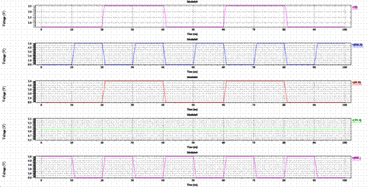
Figure 13. Output waveform of Average 8T SRAM Cell
All the above nT SRAM techniques are analyzed based on the parameters average power, delay, Read and Write access time and are presented in Table 1 and 2. From the Tables Average 8T SRAM technique gives the better performance compare with all other nT SRAM technique. Further, we proposed the Average 6.5T SRAM Cell design for better improvement in reduce number of transistors, delay, Read and Write access time compare with all the above mentioned nT SRAM Cell design techniques.
Table 1. Comparison table for various SRAM Cell design
|
Parameters |
8T SRAM |
9T SRAM |
10T SRAM |
14T SRAM |
Average 8T SRAM |
|
Average Power (Watt) |
0.0632 |
0.0756 |
0.2243 |
0.5917 |
0.0572 |
|
Delay (nano seconds) |
1.78 |
1.32 |
1.84 |
1.12 |
1.09 |
Table 2. Access Time for various SRAM Cells
|
Parameters |
8T SRAM |
9T SRAM |
10T SRAM |
14T SRAM |
Average 8T SRAM |
|
Read access time ns-nano seconds ps- pico seconds |
1.09ns |
1.12ns |
957.68ps |
1.19ns |
910.68ps |
|
Write access time (ns-nano seconds) |
1.72 |
1.27 |
1.84 |
1.12 |
1.06 |
Proposed method
Average 6.5T SRAM cell
The basic architecture of the proposed write/read-decoupled Average 6.5T SRAM is illustrated in Figure 13a and13 b. The number of transistors in each block depends on the number of bits stored in the block. This cell is capable of storing 16 bits per cell. It consists of 24 access transistors, 2 block mask transistors, 4 read transistors and 2 write transistors. Thus on an average 6.5 transistors are required to store a single bit thus takes the name average 6.5T. This is the extended version of Average 8T cell. The selection of various blocks is a trade off between several factors such as the minimum operating voltage, area constraint or minimum data retention voltage. On the basis of this analysis, to reduce the minimum operating voltage, the number of bits per block should be kept as low as possible, i.e., 14T or average-8T block should be used. On the other hand to have minimum area 16 bits per block should be used.
Calculation for Average 6.5T SRAM Cell:
Total number of transistors = 104
Each cross-coupled inverter is capable of storing 1-bit
Total number of cross-coupled inverter = 16
So, 104/16 = 6.5.
Thus on an average 6.5 transistors are required for storing a single bit, hence the name average 6.5T.
a.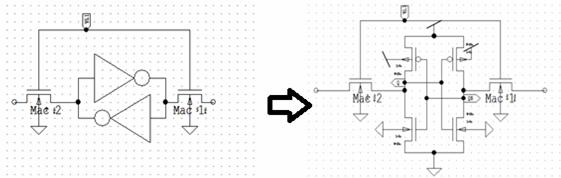
b.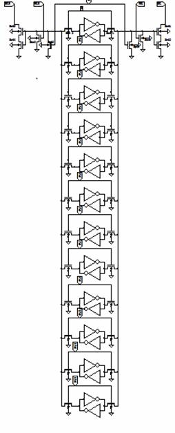
Figure 13a and b. Schematic of Average 6.5T SRAM cell
In Figure 14, the time it takes to retrieve (read) from the memory is called Read access time, which is equal to the delay between the Read request and the moment the data is available at the output. The time elapsed between a write request and the final writing of the input data into the memory is called write access time. The minimum time required between successive reads or writes is called the cycle time of the memory. This time is normally greater than the access time.
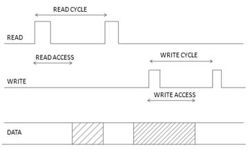
Figure 14. Memory timing parameters
READ operation
A read decoupling technique that decouples more than one bit at both Q and QB sides is proposed to improve read stability. The selection among data bits is done by the access transistors of the conventional 6T cell. There are three important features for this proposed technique. Firstly, the data-dependent-leakage is prevented. During a read operation block mask transistors, Mpd1 and Mpd2 are turned off and the access transistors of the intended bit are turned on. The stored data turns one of the read-decoupling pair transistors (Mrd1–4) on and discharges one of the pre-charged read bit-lines (RBL or RBLB). Therefore it not only minimizes but also makes it independent of the data stored in that block. Secondly, this data-independent leakage allows a large number of bits to be implemented per bit-line. Thirdly it provides a differential read port thus allowing more robust sense amplifier design.
WRITE operation
A write operation is performed by selecting the intended block and bit in the same way as a read. Based on the written data, one of the write decoupling transistors, Mwr1 or Mwr2, is turned on and pulls down the storage node in the intended bit. In addition, ultra short-segmented write in this structure improves write speed and robustness. The proposed structure is pseudo-write-tolerable for half-selected bits, thus allowing interleaving of bits. During a write operation, half-selected bits experience the same situation as read, i.e., all pull-down transistors are off and access transistors are on. The local bit-line of the proposed cell is very short, compared to the conventional 6T architecture, thereby reducing the disturbance caused by the pre-discharged local bit-line capacitance.
In Figure 15 is the output for Average 6.5T SRAM cell. Here WBL, WBLB, WL are the inputs and Q and QB are the output wave. Isolation of data storage nodes from the bit lines is possible during the read operation, which also improves the read SNM by twice in comparison with the read SNM of the conventional 6T SRAM cell.
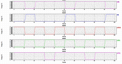
Figure 15. Output waveform of Average 6.5T SRAM Cell
Simulation results are performed using Tanner EDA (Electronic Design Automation) tool in 125nm technology with supply voltage of 5V. To establish an impartial testing environment each circuit has been tested on the same input pattern. An Average 8T SRAM cell and Average 6.5T SRAM cell are designed and the power consumption and the associated delay are compared with the existing nT SRAM cells. The Average 6.5T SRAM Cell design are consumed the average power is 0.0495Watt, delay 1.02 nano seconds, Read and Write access time are 902.54pico seconds and 1.02 nano seconds only. This proposed technique gives the better result compare with all other nT SRAM design techniques.
Conclusions
For high-speed circuit’s power consumption, delay and low leakage are the major factors. Two individual data access mechanisms for read and write operations are proposed in the average 8T cell. Charging/discharging of a single bit line is used during the write operation, which results in reduced power consumption in comparison with conventional 6T SRAM cell. In the proposed method 125nm technology is analyzed using the Tanner EDA software and the parameters such as power consumption and delay time are determined. Based on the results obtained proposed method has better performance and it is used to build the memory block.
References
1. Prabhu C. M. R., Keroh A., Singh A. K., Pin S. W., 9T balanced SRAM cell for low power operation, IEEE Symposium on Industrial Electronics & Applications, 2009, 1, p. 68-72.
2. Weste N. H. E., Kamran Eshraghian (2012), Principles of CMOS VLSI design, Pearson Education, Inc., Singapore.
3. Khare K., Azad M., Khare. N., Kulhade V. K, Deshpande P., VLSI design and analysis of low power 6T SRAM cell using cadence tool, IEEE International Conference on Semiconductor Electronics, ICSE 2008, 2008, 25-27, p. 117-121.
4. Liu Z., Kursun V., Characterization of a novel nine-transistor SRAM cell,” IEEE Trans. on Very Large Scale Integration (VLSI) systems, 2009, 16(4), p. 488-492.
5. Singh S. Sikar, Arora N., Suthar M., Leakage reduction in differential 10T SRAM cell using Gated VDD control technique", International Conference on Computing, Electronics and Electrical Technologies (ICCEET), 2012, p. 610 - 614.
6. Lu C.-Y., Chuang C.-T., A disturb-free sub-threshold 9T SRAM cell with improved performance and variation tolerance, IEEE 26th International SOC Conference (SOCC), 2013, p. 325-329.
7. Calhoun B. H., Chandrakasan A., A 256 kb sub-threshold SRAM in 65nm CMOS,”IEEE Int. Solid-State Circuits Conf. Dig. Tech. Papers, 2006, 43(1), p. 628-629.
8. Singh Jawar, Pradhan Dhiraj K., A single ended 6T SRAM cell design for ultra low voltage applications IEICE electronic express, 2010, p. 750-755.
9. Kim T.-H., Liu J., Kim C. H., An 8T sub-threshold SRAM Cell utilizing reverse short channel effect for write margin and read performance improvement, IEEE Custom Integr. Circuits Conf., 2007, p. 241-244.
10. Kim T.-H., Liu J., and Kim C. H., A voltage scalable 0.26 V, 64kb 8T SRAM with Vmin lowering techniques and deep sleep mode, IEEE J. Solid-State Circuits, 2009, 44(6), p. 1785-1795.
11. Rabaey Jan M., Low Power Design Essentials, Springer Science and business media, 21 April 2009.
12. Islam A., Hasan M., Leakage Characterization of 10T SRAM Cell, IEEE Transa. on Electron Devices, 2012, 59(3), p. 631-638.
13. Chang I. J., Park S. P., Roy K., A 32 kb 10T Sub-Threshold SRAM array with bit-interleaving and differential read scheme in 90 nm CMOS, IEEE Journal of Solid-State Circuits, 2009, 44(2), p. 650-658.
14. Kang S.-M., Leblebici Yusuf, CMOS digital integrated circuits analysis and design, McGraw-Hill International Editions, Boston, Second Edition, 1999.