Bandwidth enhanced electromagnetic bandgap structure structured closed ground monopole antenna
Modali S. S. S. SRINIVAS1, Tottempudi Venkata RAMAKRISHNA1, Boddapati T. P. MADHAV1,*, Sathuluri Venkata RAMA RAO2, Shaik ASHRAF ALI2
1 Department of ECE, K L University, AP, India
2 Department of ECE, NRI Institute of Technology, Pothavarapadu, Krishna District, AP, India
Emails: srinumodali@gmail.com; tottempudi@kluniversity.in; btpmadhav@kluniversity.in;
svr628@gmail.com; shaik.ashraf1@gmail.com
* Corresponding author, Phone: +91-9908243452
Received: May 7, 2016 / Accepted: July 17, 2016 / Published: July 31, 2016
Abstract
The primary barrier to implement microstrip patch antennas in modern broadband communication systems are their narrow bandwidth. For broadband antennas some of the characteristics are very essential like feed impedance matching, patch geometry optimization and suppression of surface waves etc. To improve impedance bandwidth low permittivity substrate with increased thickness is required. But by taking low permittivity with substrate thickness, the surface wave related problems will be raised. To overcome this problem a coplanar wave guide fed square patch monopole antenna with closed ground structure is proposed in this paper and electromagnetic band gap structure is added to the antenna design to enhance the impedance bandwidth, this being the aim of the present work. Antenna with square patch and closed ground structure is designed to resonate at dual band and by adding Electromagnetic Bandgap Structure (EBG) structure without closed ground structure in the design the modified antenna is resonating at triple band. To enhance the bandwidth and to suppress the surface waves related problems, we incorporated EBG structure and closed ground structure in the proposed antenna model. The proposed model attained bandwidth more than 10.7 GHz with impedance bandwidth of 82.3%. In this design the HFSS electromagnetic simulator tool results are in good agreement with fabricated antenna measured results over ZNB 20 vector network analyzer.
Keywords
Bandwidth Enhancement Closed Ground; Coplanar Waveguide (CPW); Electromagnetic Bandgap Structure (EBG); Monopole Antenna; Vector Network Analyzer (VNA)
Introduction
Microstrip patch antennas are one of the attractive candidates for modern communication systems to transmit and receive the data from 1m to 104 m. When used with microwave integrated circuits, the fabrication becomes simpler and low profile designs can be generated for numerous communication and military applications [1-2]. Due to surface waves, the microstrip patch antennas are suffering with low bandwidth and gain. Generally a conventional microstrip patch antenna consisting of patch on the surface of substrate material and ground plane at bottom side. The ground plane supports the propagation of TM surface waves. These waves travel along the surface that causes unnecessary end–fire radiations. With the image currents being out of phase it further causes weakening of the radiation pattern [3-5]. In addition in many of the stated applications there would be a multi-frequency operations requirement. So, the enhancement of the bandwidth and the achievement of multi frequency operation are major challenges for the microstrip patch antennas.
Surface waves are TM (Transverse magnetic) and TE (Transverse electric) modes of the substrate. These modes are characterized by waves attenuating in the transverse direction (normal to the antenna plane) and having a real propagation constant above the cutoff frequency. The phase velocity of the surface waves is strongly dependent on the substrate parameters h and εr. The lowest order TM-type mode has no cut off frequency [6-8]. It is designated as the TM0 mode .The cutoff frequencies for the higher order TMn and TEn modes are given by:
|
|
(1) |
where c is the velocity of light in free space, h is the substrate thickness and n=1, 3, 5... for TEn modes and n=0, 2,4,...for TMn modes. It will even propagate on very thin substrates having low dielectric constant values at nearly the velocity of light. The field distribution of the TE1 mode is such that it can propagate below the patch metallization, and can always be excited above the cut-off frequency. The dispersion relations for the TMn and TEn modes are given below (where μ02 = β2 - k02 and μ2 = β2 - k02εr):
¸ for TMn modes (n = 0, 2, 4, ...): εr·μ0·h + μ·h·tan(μ·h) = 0
¸ for TEn modes (n = 1, 3, 5, ...): μ0·h + μ·h·cot(μ·h) = 0.
However, one needs to know the exact value of β for the analysis of microstrip antennas. The exact value of is generally obtained using a root searching algorithm. The initial value of β is still needed in a closed form for root searching. For the TM0 mode in lossless substrates, the radial propagation constant β is real, and is bounded by 1 < β/k0 < εr. If the substrate is electrically thin, β/k0 ≈ 1. The value of β/k0 can then be obtained by assuming β/k0 = 1 + δ:
|
|
(2) |
where the infinite sum in (1) is a Taylor’s series for ![]() around the point z = β/k0
= 1. In (1):
around the point z = β/k0
= 1. In (1):
|
|
(3) |

Retaining only the dominant term α0 in (1), one can obtain [5, 6]:
|
|
(4) |
|
|
(5) |

Two-term Taylor approximation in (1) yields(5):
|
|
(6) |

This expression gives good accuracy for sh < λ0/4. If the substrate has moderate losses defined as εr·(1-j·tan(δ)), then the surface wave propagation constant will also be complex valued defined as βr = (βr-j·βi) with βi > 0. The approximate expression for β is found as (where the value of β is defined in (5) or (6)):
|
|
(7) |
For a multilayered substrate consisting of N different layers, a general formula for β/k0 for the TM0 mode has been obtained (7) it is a generalized function of (4) and is given as:
|
|
(8) |

where and are the constituent parameters of the i th layer. It is also of interest to know the value of the substrate thickness such that only the surface wave more propagates and all other modes are below cutoff. For the single-layer substrate one obtains from (a) for n=1:
|
|
(9) |
The condition for the double-layer substrate case is obtained as follows:
|
|
(10) |

Two solutions to the surface wave problem are available now. One approach is based on the micromachining technology in which part of substrate beneath the radiating element is removed to realize a low effective dielectric constant environment for antenna. In this case the power lost through surface wave excitation is reduced and coupling of power to the space engineering. In this case, the substrate is periodically loaded so that surface wave dispersion diagram presents a forbidden frequency range about antenna’s operating frequency [9-11]. Because surface waves cannot propagate along the substrate, an increased amount radiated power couples to the space wave. Also, other surface wave coupling acts like mutual coupling between array elements and interference with on hard systems are now absent.
The second solution can be addressed through electromagnetic bandgap structures (EBG). The EBG structures which are used in the microstrip patch antennas can reduce the surface wave problems and improve the gain and radiation efficiency of the antennas [12-15]. EBG is also known as an artificial magnetic conductor which can reduce the side lobes and back lobes levels with its typical structure in the design. Antennas can be designed using EBG substrate, which are selective in supporting surface waves without reversing the phase of the reflected waves [16-18]. At the same time, it provides very high impedance within a specified frequency range. Also microstrip patch antenna using electromagnetic bandgap can provide a directive radiation pattern with increase in the directivity of the main lobe and by minimizing the radiation in undesired direction. In this article the properties of electromagnetic bandgap structures are utilized in substrate design and with the help of closed ground structure.
Material and method
The design of the antenna will start with mathematical formulation and which is based on the dielectric material permittivity and resonant frequency (see the Flow Chart).
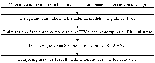
Flow Chart: Algorithm for the proposed work
Design and simulation is done with commercial electromagnetic tool High Frequency Structure Simulator (HFSS), which is based on finite element method.
A small portion of radius 1mm is removed in the form of cylinder on the FR4 substrate and filled with another dielectric material PEC. The substrate is the sandwich of FR4 and PEC, which forms the EBG structure in the substrate. Square patch and ground plane are designed with copper material of thickness 0.05 mm.
An impedance of 50 ohms is attained with the coplanar wave guide feeding technique in the design. The optimized antenna model after simulation is fabricated on FR4 substrate with thickness 4.4. The prototyped antenna is tested using vector network analyzer for validation.
Antenna geometry
Figure 1 shows the square patch antenna with closed ground structure on FR4 substrate. The overall dimension of the antenna is around 40x40x1.6 mm (Table 1). Figure 2 shows the EBG structured antenna without closed ground structure. PEC material is inserted in the FR4 substrate adjacent to patch in the cylindrical shape with height of 1.6 mm.
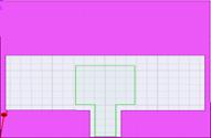


Figure 1. Antenna Iterations, (a) Square Patch with Closed Ground Structure,
(b) EBG without Closed Ground Structure, (c) EBG with Closed Ground Structure
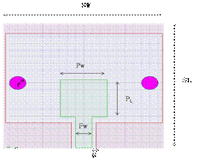
Figure 2. Proposed EBG Antenna with Closed Ground Structure
Table 1. Antenna dimensions
|
Parameter |
Sw |
SL |
Pw |
PL |
Fw |
G |
r |
|
Dimensions in mm |
40 |
40 |
6 |
6 |
3 |
0.5 |
1 |
The overall area occupied by the ground structure in the proposed antenna model is 40% less in compared with basic antenna model given in Figure 1(a).
Results and discussion
Designed antenna models are simulated using HFSS tool and their |S11|, radiation pattern and field distributions are presented in this section.
Figure 3 shows the proposed EBG antenna with closed ground structure and shows the return loss curve for the square patch antenna with closed ground structure. The basic antenna model is resonating at triple band with impedance bandwidth of 18% at 12.5 GHz, 6% at 16.5 GHz and 5.5% at 18.5 GHz.
Figure 4 shows the return loss curve for the EBG structured antenna without closed ground plane.
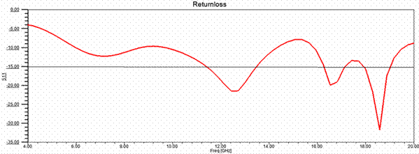
Figure 3. Return Loss Vs Frequency of Square Patch with Closed Ground Structure
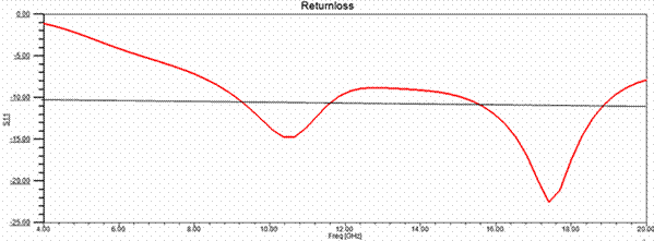
Figure 4. Return Loss Vs Frequency of EBG without Closed Ground Structure
The designed antenna is resonating at dual band with impedance bandwidth of 20% at 1.5 GHz and 22% at 17.5 GHz. The proposed EBG structured antenna with closed ground plane is shown in Figure 5.
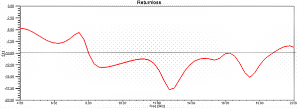
Figure 5. Return Loss Vs Frequency of EBG with Closed Ground Structure
Proposed antenna is resonating in wideband from 8 GHz to 19 GHz with bandwidth of 11 GHz. By adding EBG structure to closed ground plane we attained impedance bandwidth of 73% at center frequency of 14 GHz.
Figure 6, 7 and 8 shows the radiation pattern of the antenna models at resonating frequency, where significant consistency is achieved.
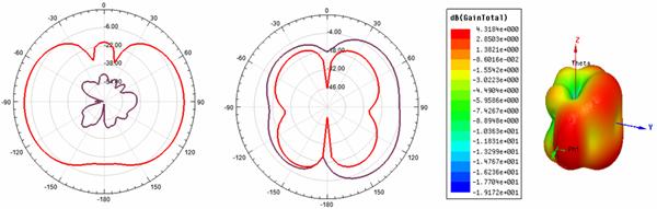
Figure 6. Radiation pattern of the square patch antenna with closed ground structure in E, H-plane and 3D
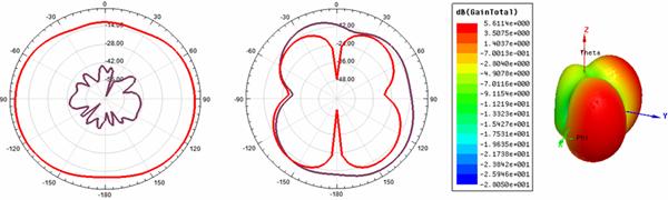
Figure 7. Radiation pattern of the EBG antenna without closed ground structure in E, H-plane and 3D
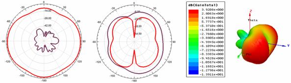
Figure 8. Radiation pattern of the proposed EBG antenna with closed ground structure in E, H-plane and 3D
The antenna displays good omnidirectional radiation patterns. Within the operating frequency band, nearly symmetric and equal radiation patterns in the E- and H-planes are achieved. In addition, the measured cross-polarization levels in E- and H-planes are generally low across the whole frequency bandwidth.
Radiation pattern is highly distorted due to the asymmetry in the configuration. The three dimensional view of the radiation pattern of the proposed antenna with antenna placement in transparent scenario can be observed from Figure 9.
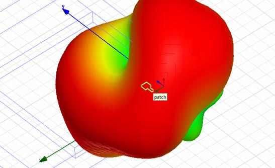
Figure 9. 3D view of the proposed antenna
The radiation field strength in different directions can be observed from this appearance. Asymmetry in the structure induces an asymmetric field distribution in the ground plane as shown in Figure 10.
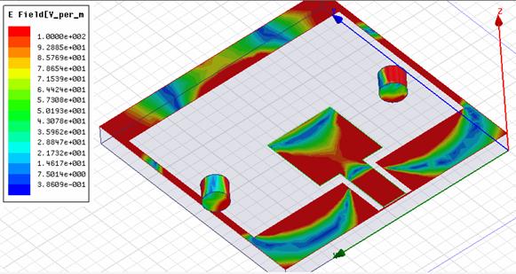
Figure 10. E-Field distribution of the proposed antenna at 14GHz
Feed line and lower half of the patch surface is showing more field intensity compared with ground plane. The proposed antenna and base model are fabricated on FR4 substrate of dielectric constant 4.4 and thickness 1.6 mm.
Figure 11 shows the prototyped antennas of model 1 and model 3.
|
|
|
|
a) |
b) |
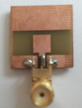
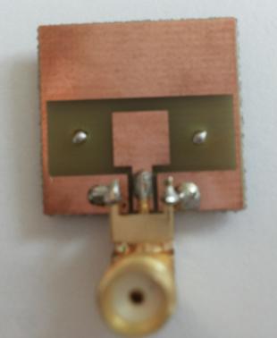
Figure 11. Prototyped Antennas, (a) Square Patch Closed Ground Antenna,
(b) EBG structured Closed Ground Antenna
A small spot on substrate i.e., EBG can be observed on both sides of the patch. Coplanar wave guide feeding is used in the design and SMA connector is connected to support 50 ohm impedance in the fabricated models.
ZNB 20 Vector network analyzer is used to analyze the reflection coefficient results of the prototyped antenna. Figure 12 shows the measured reflection coefficient of the proposed EBG structured closed ground antenna.
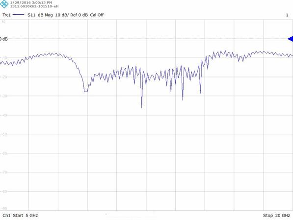
Figure 12. Measured Return loss of proposed antenna on ZNB 20 VNA
Antenna is showing similar kind of reflection coefficient results of simulated model and good agreement can be observed between HFSS and VNA. Antenna is showing almost 11 GHz bandwidth in the desired operating band.
Conclusions
The fabricated antenna results on VNA are in good agreement with the simulated results. Antenna 1 with square patch and closed ground structure is resonating at triple band with impedance bandwidth of 18% at 12.5 GHz, 6% at 16.5 GHz and 5.5% at 18.5 GHz. Antenna 2 with EBG structure and without closed ground plane is resonating at dual band with impedance bandwidth of 20% at 1.5 GHz and 22% at 17.5 GHz. The proposed EBG structured antenna with closed ground plane is resonating in the wideband from 8 GHz to 19 GHz with bandwidth of 11 GHz. By adding EBG structure to closed ground plane we attained impedance bandwidth of 73% at centre frequency of 14 GHz.
The proposed antenna model is showing gain more than 4 dB in the operating band with efficiency greater than 85%. The results obtained from the current antenna are most suitable for the stable gain wideband communication systems.
Acknowledgements
Authors like to express their gratitude towards the department of ECE and management of K L University and management of NRI Institute of Technology for their support and encouragement during this work. Further Madhav likes to express his gratitude towards FIST grant from DST (SR/FST/ETI-316/2012).
References
1. Rong Zheng Q., Fu Y., Chang Yuan N., A Novel Compact Spiral Electromagnetic Band-Gap (EBG) Structure, IEEE Transactions on Antennas and Propagation, 2008, 56, p.1656-1650.
2. Madhav B. T. P., Krishnam Naidu Yedla G. S., Kumar K. V. V., Rahul R., Fractal aperture EBG ground structured dual band planar slot antenna, International Journal of Applied Engineering Research, 2014, 9(5), p. 515-524.
3. Madhav B. T. P, Pisipati V. G. K. M., Habibulla K., Ujwala D., Fractal shaped Sierpinski on EBG structured ground plane, Leonardo Electronic Journal of Practices and Technologies, 2014, 25, p. 26-35.
4. James J., Hall P., Handbook of microstrip antennas, IEEE Electron. Waves Series, 28, 1988.
5. Madhav B. T. P, Manikanta A. Prasanth, Sreeramineni Prasanth, Batchu Mohan Sai Krishna, Devani Manikantha, Usirika Sharmila NagaSai, Analysis of Defected Ground Structure Notched Monopole Antenna, ARPN Journal of Engineering and Applied Sciences, 2015, 10(2), p. 747-752.
6. Srinivas M. S. S. S, Ramakrishna T. V., Madhav B. T. P, Bhagyalakshmi N., Madhavi S., Venkateswarulu K., A Novel Compact CPW Fed Slot Antenna with EBG Structure, ARPN Journal of Engineering and Applied Sciences, 2015, 10(2), p. 835-841.
7. Narasimha Nayak V., Madhav B.T.P, Sai Divya R., Nava Sai Krishna A., Rohith Ramana K., Mounika D., Compact Microstrip Rectangular Edge Fed Antenna with DGS Structure, International Journal of Applied Engineering Research, 2015, 10(10), p. 24331-24348.
8. Gonzalo R., Maagt P., Sorolla M., Enhanced patch-antenna performance by suppressing surface waves using photonic-bandgap substrates, IEEE Trans. Microwave Theory Technology., 1999, p. 2131-2138.
9. Madhav B. T. P., Naga Vaishnavi D., Vanaja G., Jayasree G., Mounika S., Design and analysis of metamaterial antenna with EBG loading, Far East Journal of Electronics and Communications, 2015, 14(2), p. 127-136.
10. Madhav B. T. P., Mounika Sanikommu M. N. V. S., Pranoop K. S. N., Manikanta Chandra Bose, Sriram Kumar B., CPW Fed Antenna for Wideband Applications based on Tapered Step Ground and EBG Structure, Indian Journal of Science and Technology, 2015, 8(9), p. 119-127.
11. Ramkiran D. S., Madhav B. T. P., Sahithi Krishnaveni Grandhi, Amara Venkata Sumanth, Sri Harsha Kota, Leela Krishna Boddu, Compact Microstrip Band pass Filter with Defected Ground Structure, Far East Journal of Electronics and Communications, 2015, 15(1), p. 75-84.
12. Sauleau R., Coquet P., Input impedance of electromagnetic bandgap resonator antennas, Microwave and Optical Technology Letters, 2004, 41(5), p. 369-375.
13. Madhav B. T. P., Habibulla Khan, Sarat Kotamraju K., Circularly Polarized Slotted Aperture Antenna With Coplanar Waveguide Fed for Broadband Applications, Journal of Engineering Science and Technology, 2016, 11(2), p. 267 – 277.
14. Mohan Reddy S. S., Mallikarjuna Rao P., Madhav B. T. P., Asymmetric Defected Ground Structured Monopole Antenna for Wideband Communication Systems, International Journal of Communications Antenna and Propagation, 2015, 5(5), p. 256-262.
15. Bhavani K. V. L., Habibulla Khan, Madhav B. T. P., Multiband Slotted Aperture Antenna With Defected Ground Structure For C And X-Band Communication Applications, Journal of Theoretical and Applied Information Technology, 2015, 82(3), p. 454-461.
16. Madhav B. T. P., Jayasree Gogineni, Harini Appana, Jyothi Prathusha Chennam, Durga Sai Sruthi Thota, Priyanka Kotte, Analysis of Compact Coplanar Waveguide Fed Slot Antenna with EBG Structure, Spaces-2015, p. 219-225.
17. Madhav B. T. P., Mounika Sanikommu, Pranoop M. N. V. S., Manikanta Chandra Bose K. S. N., Sriram Kumar B., CPW Fed Antenna for Wideband Applications based on Tapered Step Ground and EBG Structure, Indian Journal of Science and Technology, 2015, 8(S9), p. 119-127.
18. Agi K., Mojahedi M., Minhas B., Schamiloglou E., Malloy K., The effects of an electromagnetic crystal substrate on a microstrip patch antenna, IEEE Transactions on Antennas and Propagations, 2002, 50(4), p. 451-456.